Electronics explained.Transistor circuits
488 33 100KB
English Pages 11
Recommend Papers

![Electronics Microelectronic Circuits [5 ed.]](https://ebin.pub/img/200x200/electronics-microelectronic-circuits-5nbsped.jpg)

![Milman's electronics devices and circuits [3 ed.]
9780070700215, 0070700214](https://ebin.pub/img/200x200/milmans-electronics-devices-and-circuits-3nbsped-9780070700215-0070700214.jpg)
![Device Electronics for Integrated Circuits [3rd ed.]
9780471428770, 0471428779](https://ebin.pub/img/200x200/device-electronics-for-integrated-circuits-3rdnbsped-9780471428770-0471428779.jpg)


![Electronics Fundamentals: Circuits, Devices and Applications: Pearson New International Edition [8th edition]
1292025689, 9781292025681](https://ebin.pub/img/200x200/electronics-fundamentals-circuits-devices-and-applications-pearson-new-international-edition-8th-edition-1292025689-9781292025681.jpg)
- Similar Topics
- Technique
- Electronics
File loading please wait...
Citation preview
Electronics Explained: Transistor Circuits Investigating a common-emitter amplifier 1 Assemble the amplifier circuit shown below. Use a low power signal bipolar transistor.
2 Use a double-beam oscilloscope to monitor the voltages at W and C. If all is well, the voltage at C should fall as the voltage at W rises. 3 Set W to 0 V and slowly increase it until C starts to fall below +5 V. Note the value of the voltage at W. Then continue to increase the voltage at W until C hits 0 V and the transistor saturates. Note the new voltage at W. 4 Use the data from step 3 to calculate a value for the voltage gain of the circuit. Don't forget the sign. 5 Adjust the potentiometer so that C sits at +2.5 V. This should give the amplifier optimum bias. 6 Use a signal generator to feed a 1 kHz sine wave with a peak value of 200 mV into the amplifier. Trigger the oscilloscope on the signal at the output. Sketch waveforms of the signals at IN, W, B, C and OUT. Don't forget to show the scales of the voltage and time axes. 7 Use the peak values of the input and output waveforms to calculate a value for the voltage gain. How does it compare with your value calculated in step 4? 8 Investigate the effect on the output waveform of altering the d.c. voltage at W. 9 Return the bias to its original optimum setting (step 5). Without altering anything else, note what happens when you replace your transistor with different ones.
Michael Brimicombe 12/02/02
Electronics Explained: Transistor Circuits 10 Insert the original transistor. Remove the potentiometer. Use a 22 k bias from the collector, as shown below.
resistor to provide
11 Measure the voltage gain of your new amplifier. 12 Note what happens now to the voltage gain and the bias if you replace the transistor with others.
Michael Brimicombe 12/02/02
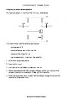
Electronics Explained: Transistor Circuits Designing an emitter-biased amplifier Your task is to design an amplifier similar to the one shown below.
The amplifier must have the following specifications: a voltage gain of -5 operate off supply rails at +5 V and -5 V have an emitter resistor of 100 use transistors with a current gain of at least 100 1 Do all of the design calculations. 2 Assemble the circuit. 3 Test it with a 1 kHz sine wave of peak value 500 mV. 4 Record sketch waveforms of the signals at the base, emitter and collector of the transistor. Use them to measure the voltage gain of the amplifier. 5 Verify that replacement of the transistor with others does not significantly alter the operation of the amplifier circuit.
Michael Brimicombe 12/02/02
Electronics Explained: Transistor Circuits The effects of negative feedback 1 Assemble the circuit shown below, using one NOT gate from a 4069 i.c. Run it off supply rails of +5 V and -5 V instead of the usual +5 V and 0 V.
2 Use a signal generator to inject a 1 kHz test signal at the input. Use a double-beam oscilloscope to monitor the signals at the input and output. If all is well, the output should be at least ten times bigger than the input. 3 Explore the effect of increasing and decreasing the amplitude of the input signal. Admire the distortion of the output signal for large amplitude input signals. 4 Adjust the amplitude of the input signal until the output has a peak value of 1.0 V. Measure the amplitude of the input signal. Hence determine a value for the open-loop gain A of the amplifier. 5 Now use a couple of 10 k resistors to provide negative feedback, as shown below. The block marked NOT gate amplifier is the entire circuit shown above.
6 Check that the closed-loop gain G is now -1, with very little distortion (even at large amplitudes). 7 Use the following values of R in turn: 4.7 k , 2.2 k , 1.0 k , 470 and 220 . Measure the value of the closed-loop gain G each time, making sure that the output is not saturated. 8 Detailed theoretical analysis of the circuit suggests that G = -1 104/R when G is much less than A. Is this supported by your results?
Michael Brimicombe 12/02/02
Electronics Explained: Transistor Circuits Exploring the MOSFET characteristic 1 Assemble the circuit shown below. Use a 2N7000 MOSFET.
2 Use a double-beam oscilloscope to monitor the voltages at the gate and drain of the MOSFET. If all is well, the voltage at the drain Vd should fall as the voltage at the gate Vg rises. 3 Measure the voltage at the drain for the gate voltages shown in the table. Vg /V 0.0 1.0 2.0 2.2 2.4 2.6 2.8 3.0
Vd /V 5.0
4 By considering the voltage drop across the 100 current Id for each value of the drain voltage Vd.
Id /mA 0.0
resistor, calculate a value for the drain
5 Use your results to plot a graph to show how the drain current depends on the gate voltage. Use it to obtain values for the threshold voltage Vth and transconductance gm of your MOSFET.
Michael Brimicombe 12/02/02
Electronics Explained: Transistor Circuits A MOSFET follower 1 Assemble the voltage follower circuit shown below.
2 Use a double beam oscilloscope to monitor the voltages at the wiper and source. Use the potentiometer to vary the voltage at the gate. If all is well, the voltage at the source should rise from -5 V to about +3 V as the gate is raised from -5 V to +5 V. (The voltage at the gate should equal the voltage at the wiper.) 3 Set the wiper/gate voltage to -5.0 V. Measure the source voltage. Increase the gate voltage in steps of 1.0 V, measuring the source voltage each time. Plot the results on a grid like the one shown below.
4 Use the graph to state the voltage gain of the circuit when a.c. signals are placed at in. Suggest an optimum value for the d.c. voltage at the gate. Use the potentiometer to set the gate to this optimum voltage. Do not change it from now on.
Michael Brimicombe 12/02/02
Electronics Explained: Transistor Circuits 5 The block diagram below shows how you can measure the input and output impedance of the circuit. Rin is a resistor in series with the follower input, and Rout is a load resistor at the output.
6 Verify that the input impedance of the voltage follower is 4.7 M
as follows.
Make Rin and Rout both 47 k . Adjust the signal generator so that the oscilloscope displays a 1 kHz sine wave with an amplitude of 1.0 V. Replace Rin with 470 k and 4.7 M in turn. The latter should halve the amplitude of the signal displayed on the screen. This means that the input impedance of the voltage follower is about 4.7 M . 7 Measure the output impedance of the voltage follower as follows. Note the amplitude of the signal displayed on the oscilloscope screen when Rin is left at 4.7 M . Replace Rout with 4.7 k , 2.2 k , 1.0 k , 470 , 220 and 100 amplitude of the signal displayed on the screen each time.
in turn, noting the
Use the results to estimate the output impedance of the voltage follower. 8 The block diagram below shows one way of demonstrating the benefits of a large input impedance for a voltage follower. Try it out.
Michael Brimicombe 12/02/02
Electronics Explained: Transistor Circuits A MOSFET amplifier 1 Assemble the amplifier circuit shown below. Use a 2N7000 MOSFET.
2 Use a double-beam oscilloscope to monitor the voltages at the wiper and the drain. If all is well, the voltage at the drain should fall as the voltage at the wiper (and gate) rises. 3 Set the wiper to 0 V and slowly increase it until the drain starts to fall below +5 V. Note the value of the wiper voltage. Then continue to increase the wiper/gate voltage until the drain hits 0 V and the MOSFET saturates. Note the new gate voltage. 4 Use the data from step 3 to estimate a value for the voltage gain of the circuit. Don't forget the sign. 5 Adjust the potentiometer so that the drain sits at +2.5 V. This should give the amplifier optimum bias. 6 Use a signal generator to feed a 1 kHz sine wave with a peak value of 100 mV into the amplifier. Trigger the oscilloscope on the signal at the output. Sketch waveforms of the signals at IN and OUT. Don't forget to show the scales of the voltage and time axes. 7 Use the peak values of the input and output waveforms to calculate a value for the voltage gain. How does it compare with your value calculated in step 4? 8 Investigate the effect on the voltage gain of changing the drain resistor Rd. Use the values shown in the table. You will need to adjust the bias each time. Make sure that the signal is small enough so that the amplifier is not saturated! drain resistor 100 220 470
voltage gain
9 The voltage gain G should be given by the formula G = -gmRd. What value does the data suggest for the transconductance gm of your MOSFET?
Michael Brimicombe 12/02/02
Electronics Explained: Transistor Circuits 10 Remove the potentiometer. Use the 4.7 M shown below.
resistor to provide bias from the drain, as
11 Measure the voltage gain of your new amplifier. 12 Note what happens now to the voltage gain and the bias if you replace the MOSFET with others.
Michael Brimicombe 12/02/02
Electronics Explained: Transistor Circuits MOSFET resistors You are going to find out how the drain-source resistance of a MOSFET depends on its gate-source voltage. 1
Assemble the circuit shown below. It uses a 2N7000 MOSFET as the pull-down resistor of a non-inverting amplifier.
2
Check that point W is at +50 mV. If all is well, the voltage at point Y should go from +50 mV to +3 V as the potentiometer is adjusted.
3
The gate voltage fixes the drain-source resistance Rds of the MOSFET. Because of the negative feedback around the op-amp, X sits at a steady +50 mV and the voltage gain G of the op-amp circuit is given by G = 1 + 470 Rds .
4
Measure the voltage at the gate Vgs required to obtain the op-amp output voltages Vy shown in the table. Vy / V 0.10 0.20 0.40 0.80 1.60
5
Vgs / V
G
Rds /
Complete the table. Plot a graph to show how the drain-source resistance of the MOSFET depends on its gate-source voltage.
Michael Brimicombe 12/02/02
Electronics Explained: Transistor Circuits Using analogue switches This experiment should give you some idea of the usefulness of analogue switches. 1
The circuit below uses the four analogue switches of a 4066 i.c. to place four different voltages at OUT, depending on the logic signals at P, Q, R and S.
2
Assemble the circuit shown above. All four pull-down resistors for the analogue switch control inputs which need to be at least 10 k . The pull-down resistors for the push switches can have any value.
3
If all is well, the voltage at OUT should be 0 V, 1 V, 2 V or 3 V depending on which one of P, Q, R or S is pulled high.
4
Design a logic system using NOT and AND gates which will allow the circuit to obey this table. B and A are digital signals from the two push switches. B 0 0 1 1
5
A 0 1 0 1
P
Q
R
S
OUT 0V 1V 2V 3V
Assemble the logic system. Test the whole circuit. It performs the function of a digital-to-analogue converter.
Michael Brimicombe 12/02/02