Signaling in high-performance memory systems
373 67 412KB
English Pages 30
Recommend Papers

![Notch Signaling in Embryology and Cancer: Notch Signaling in Cancer [1st ed.]
9783030550301, 9783030550318](https://ebin.pub/img/200x200/notch-signaling-in-embryology-and-cancer-notch-signaling-in-cancer-1st-ed-9783030550301-9783030550318.jpg)


![Neurochemical Systems and Signaling: From Molecules to Networks (2023) [1 ed.]
0367210622, 9780367210625](https://ebin.pub/img/200x200/neurochemical-systems-and-signaling-from-molecules-to-networks-2023-1nbsped-0367210622-9780367210625.jpg)
![Neurotransmitters in Plant Signaling and Communication [1st ed.]
9783030544775, 9783030544782](https://ebin.pub/img/200x200/neurotransmitters-in-plant-signaling-and-communication-1st-ed-9783030544775-9783030544782.jpg)
File loading please wait...
Citation preview
Signaling in High-Performance Memory Systems John Poulton Research Professor Department of Computer Science University of North Carolina at Chapel Hill [email protected] http://www.cs.unc.edu/~jp
ISSCC 1999 Signaling in High-Performance Memory Systems
1 of 59
What's a Signaling System? 1 Transmitter
2 Transmission Line
3 Receiver +
Data In
− 4 Terminator
Data Out
VRef
5 Clock(s)
1. Transmitter encodes data as voltage/current signal levels onto the line 2. Transmission line delivers the signal to the receiver 3. Receiver compares signal with reference to recover data 4. Terminator removes signals from line, once they're received 5. Clocks tell transmitter when to drive a new signal, receiver when to sample For this discussion, we'll assume • binary (two-level) signaling • direct encoding ( e.g. VHi = "1", V Lo = "0") ISSCC 1999 Signaling in High-Performance Memory Systems
2 of 59
A Bus has • multiple transmitters and receivers ("drops"), often paired up as transceivers • transceivers share a common transmission line • any one drop may send; any (or all) drops receive at a given time
This is not a bus:
This isn't a bus, either:
...it's a linear network.
...it's a bidirectional link. ISSCC 1999 Signaling in High-Performance Memory Systems
3 of 59
Outline 5
28
29
35 36
55 56
• Transmission Lines ° Impedance, propagation, reflection ° Impedance discontinuities ° Termination methods ° Loss mechanisms ° Cross-talk, modes, impedance matrices ° Typical properties of PC-board T-lines
• Signaling Methods ° Voltage-mode vs Current-mode ° Single-ended vs Differential ° References ° Clocking
• Bus-based Signaling Systems ° Problems: lowered Z 0, v, f c ° CMOS , voltage-mode signaling ° SSTL & SLDRAM ° Open-drain systems, BTL, GTL, etc ° RAMBUS ° Summary
• Alternative Signaling Approaches ° Future Prospects ° Serial Links
57
• Wrapup, Questions, Discussion ISSCC 1999 Signaling in High-Performance Memory Systems
4 of 59
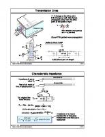
Transmission Lines If I,V change at the drive point, B,E change as well; disturbance propagates away from the drive point at the speed of light E
v= Dielectric ( ε,µ ) I
1 c ≈ εµ εr
x
B
IF the dielectric is homogeneous and µ = µ (as usual) 0
V
dx
(Quasi-TEM guided wave propagation) I(x)/2
C=
− − −−
Q V
L=Φ I
...leads to circuit model
Ldx Rdx
I(x) + + + + I(x+dx)
dV R= I
+ + ++
V(x)
Cdx
Gdx
V(x+dx) − − −−
I(x)/2
G=
dI V
dx
L,R,C,G are per unit length
ISSCC 1999 Signaling in High-Performance Memory Systems
5 of 59
Characteristic Impedance Semi-infinite line
Impedance is some value Z 0 Still semi-infinite
Peel off dx worth of line; impedance still Z 0 dx Ldx Rdx
So, original line looks like this:
Z0
Z 0 = Rdx + jωLdx +
Cdx
Gdx
Z0
1 jωCdx + Gdx + 1/Z0
(Z 0–Rdx–jωLdx)( jωCdx + Gdx + 1/ Z0) = 1 Z0(G+ jωC)dx – (R+ jωL)dx(G+ jωC)dx –
Z0 =
R+jωL = G+jωC
(R+jωL)dx =0 Z0
L when R=G=0 C
Impedance of a (near-) lossless line is frequency independent and real--just a resistance!
ISSCC 1999 Signaling in High-Performance Memory Systems
6 of 59
Propagation Constant Ldx Rdx
I(x)
–(R+jωL)V(x) ∂V(x) = –(R+jωL)I(x) = ∂x Z0
Z0
V(x)
Gdx V(x+dx)
Cdx
∂V(x) 1/2 = –[(G+jωC)(R+jωL)] V(x) ∂x V(x) = V(0) e–Ax ; A = [(G+jωC)(R+jωL)]
1/2
A = (jωRC + jωGL –ω2 LC) 1/2 = jω LC ( 1–jRC+GL ) Taylor exp. ωLC = jω LC ( 1–jRC+GL ) 2ωLC 1/2
V(x)
GZ 0 = jω LC + R + 2 2Z0 Phase change along line, where wave velocity is
v=
V(0)
1 = 1 LC εµ
e –(α R + α D )x 2πv ω
(x) = V(0) e– jω LCx e –(α R + α D)x GZ 0 Attenuation αR = R αD = 2Z 0 2 conductor loss
Re
V(x) V(0) distance x along line
dielectric loss
ISSCC 1999 Signaling in High-Performance Memory Systems
7 of 59
Characteristic Impedance of Some Typical Lines h
w
a s c
R DC =
2ρ wh
C = εw s µ s Z0 = ε w
r
s
s
w
h
s
b
ρ ρ + πa2 π(c 2 –b 2) C = 2πε log(b/a) µ log(b/a) Z0 = ε 2π R DC =
r
2ρ πr2 C = πε log(s/r) µ log(s/r) Z0 = ε π R DC =
ρ πr2 C = 2πε log(2s/r) R DC =
Z0 =
µ log(2s/r) ε 2π
R DC =
ρ wh
2πε C ≈ εw s + log(4s/h) Z0 =
εµ C
Good only for homogeneous dielectrics, where L = εµ/C Caveats: 1. Approximations only, useful for 1rst-order estimates; do NOT use these formulas for anything serious! Fire up your field solver... 2. Good only for homogeneous dielectrics; PC-board microstrips are not homogeneous. 3. Since µ = µ0 for many dielectrics,
µ ε =
µ0 377Ω 1 ε0 • ε r = ε r
Main thing to note: Z 0 is always a function of ratios of dimensions! ISSCC 1999 Signaling in High-Performance Memory Systems
8 of 59
RC vs LC Behavior Ldx Rdx Cdx
In many situations, it's reasonable to set G=0 (dielectrics are pretty good for many signaling systems) What about R? If jωL > R, then mainly an LC line Every line has some frequency f0 = R 2πL below which it's RC and above which it's LC
ISSCC 1999 Signaling in High-Performance Memory Systems
9 of 59
RC & LC Approximations
A typical on-chip wire: 0.5µ 0.5µ SiO 2, εr = 3.9
2µ
L = 0.6 nH/mm C = 73 fF/mm Rdc = 120 Ω/mm f0 = 32 GHz
The RC model works for CMOS! (...well, mostly...)
A typical PC-board wire: 5 mil
6 mil 0.7mil
"FR-4", εr = 4.5
L = 0.5 nH/mm C = 104 fF/mm Rdc = 0.008 Ω/mm f0 = 2.5 MHz
6 mil
The LC model is OK for PC board traces (mostly... R = R(f) from skin effect)
ISSCC 1999 Signaling in High-Performance Memory Systems
10 of 59
Signal Returns L
R
Impedance of line AND it's return!
C
G
In striplines, return current in planes is concentrated near signal conductor, so return impedance is significant
ISSCC 1999 Signaling in High-Performance Memory Systems
11 of 59
Skin Effect Skin depth:
E δ=
ρ πfµ
depth into conductor where E falls to 1/e of surface value
Skin-depth frequency: fs =
4ρ 4ρ = 2 πµs π µ 0 s2 non-magnetic conductors
s
approximation!
frequency at which skindepth equals half the conductor thickness
ISSCC 1999 Signaling in High-Performance Memory Systems
12 of 59
Conductor Loss R(f) = R DC
f fs
α C(f) =
f fs
DC
2Z 0
P(1m) ) P(0) V(1m) = 20 log10 ( ) V(0) = 8.686 • α C
Attn (dB/m) = 10 log 10 (
(x) = e–αCL V(0)
RDC must include returns
Some typical signal conductors Conductor
fs
Attn (@ 1GHz)
RG-223/U
22.5 KHz
0.5 dB/m
5-mil, 0.5 Oz PCB trace
56 MHz
6 dB/m
µ x 0.5µ µ 0.5µ on-chip wire 113 GHz
V(6") = 0.90 @ 1GHz V(0) possibly a concern for busbased memory signaling
same as DC!
ISSCC 1999 Signaling in High-Performance Memory Systems
13 of 59
Dielectric Loss 1010 Hz (µwave)
1013 Hz (infrared)
1015 Hz (light)
εr dipolar
ionic
electronic
G(ω)
...so, can define tanδ = G ωC GZ 0 2π f C tanδ L/C αD = = 2 2 = π f tanδ LC
freq
αD =
"RF" range:
π εr f tanδδ c
G ≈ k•ω
only for homogeneous dielectrics!
Some typical PC Board Dielectrics εr
Dielectric "FR-4"
$
GETEK $.$ Teflon
αD @1GHz tanδδ 8.86α
4.7 0.035
7.0 dB/m
3.9 0.010
1.8 dB/m
$$$ 2.25 0.001
V(6") = 0.89 @ 1GHz V(0) so, possibly a concern for memory interconnect
0.14 dB/m
ISSCC 1999 Signaling in High-Performance Memory Systems
14 of 59
Terminators Real lines (PCB traces, cables) are fairly low-loss • Good news: signals get from here to there with little attenuation • Bad news: if the signals aren't removed, they'll bounce around and interfere with later signals (a.k.a, inter-symbol interference ). The terminator gets rid of the signal once it's received To see what happens at terminations (and other discontinuities), useful to introduce a mythical voltage generator that represents the traveling wave. Terminator
IF = V/Z 0 V IF 2•V
Z0
V
ISSCC 1999 Signaling in High-Performance Memory Systems
15 of 59
General Terminations Mythical voltage divides across line & terminator producing terminator current...
VT = 2V•
ZT Z 0+Z T
IF = V/Z 0
V I T = T = 2V Z T Z0+Z T
ZT
V Z0 2•V
Σ currents into output node = 0
Reflection Coefficient (Γ)
I R = I F – I T = V – IT Z0 V(Z T– Z 0 ) = Z 0(Z T + Z 0) I V Z – Z0 Γ = R= R = T I F VF Z T + Z 0
This situation is highly desirable; forward wave is completely absorbed at the receiver.
IF IR
IT ZT
Γ is +
ZT > Z 0
Γ is −
ZT < Z 0
Γ is 0!
ZT = Z 0
VT
ISSCC 1999 Signaling in High-Performance Memory Systems
16 of 59
Source Termination Can just as well put the terminator at the transmitter (source, or series termination) Termination Z0
V/2 0
Forward Wave
V/2
Γ = +1
tf
V V/2
Reverse Wave
V/2
V
V
V/2
V/2
V/2
0
0
0 t=0
t=tf t=2t f
t=tf t=2t f
t=0 reflected "1"
VOUT
tf
V
Open circuit
V
t=0
V
t=t f t=2t f reflected "0"
VIN
VOUT t=0
Tx Current 0
What happens when pulse width < t f ??
t=0
t=t f
t=t f
Current only flows when tx opposes reflected wave, so low power!
t=2t f
ISSCC 1999 Signaling in High-Performance Memory Systems
17 of 59
Imperfect Terminations: Capacitance Suppose your 'perfect' terminator is shunted by a capacitor (as it usually is!!): ZS Z0
VIN
C
VOUT
Z0 2•V
Z0
Bandwidth is limited by cutoff frequency of Thévenin network, f0 = 1 πZ0 C If the forward wave is a fast-rise edge, the capacitor generates a large reflection: V IN
V OUT t=t f
V
Thévenin Equiv. C
If the transmitter isn't perfectly matched (Z S = Z 0), the reflection bounces off the transmitter and heads toward the receiver again.
t = Z0C/2
t=0
Z0 /2
C
t=2•t f
ISSCC 1999 Signaling in High-Performance Memory Systems
18 of 59
Managing Reflections with Capacitive Termination What happens as you increase the risetime?? V (volts)
1 0.8 0.6 0.4 0.2 0
V (volts)
VIN
1 0.8 0.6 0.4 0.2 0
Z0=50Ω, t f=2.5nsec VOut 0
1
V (volts)
2
3
4 5 6 Time (nsec)
7
8
9
1
2
3
4 5 6 Time (nsec)
1 0.8 0.6 0.4 0.2 0
7
8
9
10
trise = 4•(Z 0C/2) 0
1
2
3
4 5 6 Time (nsec)
1 0.8 0.6 0.4 0.2 0
7
8
9
10
trise = 10•(Z 0C/2) 0
1
2
3
4 5 6 Time (nsec)
7
8
9
10pF
V IN
VOut
10
trise = 1•(Z 0C/2) 0
V (volts)
trise = 0.5•(Z 0C/2)
10
As a rule of thumb, if you want reflection to be (1/n)th of signal, risetime should be n•Z 0C/2. ...or, need to terminate the transmitter as well as the receiver, to absorb reflections. Series termination works fine (no terminator at rx), but bandwidth will be halved, i.e., 1/(2πZ0C) instead of 1/( πZ0C)
ISSCC 1999 Signaling in High-Performance Memory Systems
19 of 59
Imperfect Terminations: Stubs Suppose the terminator isn't actually at the end of the line?? Reflection,
Transmission,
Γ = -1/3
1−Γ = 2/3
tf = 2 nsec
ZS
tst = 0.25nsec Z0
VIN
VOUT
Z0
VOUT
Volts
VSTUB
Volts
VIN
Volts
...but that's just the first bounce! 1.2 1 0.8 0.6 0.4 0.2 0 1.2 1 0.8 0.6 0.4 0.2 0 1.4 1.2 1 0.8 0.6 0.4 0.2 0
2•V
Z0
Z0
VSTUB
As with cap's, can mitigate the evil effects of stubs with risetime control. 1.2 1 0.8 0.6
tr = 5•t st
0.4 0.2 0
1
2
3
4 5 6 Time (nsec)
7
8
9
10
0 0
1
2
3
4
5
6
7
8
9
10
ISSCC 1999 Signaling in High-Performance Memory Systems
20 of 59
A Typical Stub Termination
Z0=75Ω Z0=50Ω tf=40psec tf=40psec
Z0=50Ω tf=1nsec
0.2pF 5nH trace
50Ω
bond wire
pkg
land Stub! ~ 200 psec
Signal at Tx (0.25nsec edge) Internal signal at Rx pad & at terminator
1.2 1 0.8 0.6 0.4 0.2 0 1.6 1.4 1.2 1 0.8 0.6 0.4 0.2 0
2pF pad & rx
Generally, you'd probably like to avoid this type of behavior. • Edge-rate control • Careful board layout • Advanced packaging • On-chip termination
pad term
0
0.5
1
1.5
2
2.5
3
3.5
4
4.5
5
ISSCC 1999 Signaling in High-Performance Memory Systems
21 of 59
T-Line Discontinuities Capacitive discontinuity: works pretty much like the capacitively shunted terminator
Inductive discontinuity: the complementary behavior to the capacitive one
Impedance discontinuity: with Z' < Z 0
Z0
Z ' < Z0
Z0
Impedance discontinuity: with Z' > Z 0
Z0
Z ' > Z0
Z0
One thing they have in common: they're all low-pass! ISSCC 1999 Signaling in High-Performance Memory Systems
22 of 59
Stub Discontinuities Z0
Z0
Z0
Z0
Open Stub with Z ' < Z 0
Z0
Z0
Open Stub with Z ' = 0.5•Z 0
ISSCC 1999 Signaling in High-Performance Memory Systems
23 of 59
Some Common Discontinuities
Vias are small capacitive discontinuities (C ~ 0.1pF typically)
Ground-plane slots are inductive discontinuities (also pretty good antennas!). Often created unintentionally in dense fields of vias.
Z < Z0
Multi-drop signals introduced stub discontinuities.
Trace squeezes introduce in-line low-impedance section.
..or..
Connectors introduce impedance discontinuities, often modeled with a combination of lumped elements.
ISSCC 1999 Signaling in High-Performance Memory Systems
24 of 59
I1
Field distribution depends on relative directions of currents in neighboring lines...
I1 I2
I2
...and so does impedance!
"Odd-mode" excitation
impedance =
L+ Lm C Cm
Z Odd =
L– Lm C + Cm
Z Lm
L
C
Z0
L
Cm C
distance between lines ISSCC 1999 Signaling in High-Performance Memory Systems
25 of 59
Crosstalk V fe Z0
Z0
Cm
Vin
Z0 Z0
Vne
Lm
capacitive coupling
inductive coupling
IF lines are homogeneous AND all ports are terminated... equal, when homogeneous
V in Kne•V in V ne V fe t=0
t=tf
t=2•t f
Vne 1 C m L m C = ( + )= m Vin 4 C L 2C V C L K fe = fe = 1 ( m – m ) = 0 Vin 4 C L
K ne =
In inhomogeneous lines, far-end crosstalk gets worse with • faster edges • longer lines ISSCC 1999 Signaling in High-Performance Memory Systems
26 of 59
solder-mask & air up here FR-4 down here
v c/ εr C Lm ≠ C L
Z0
Microstrips aren't homogeneous; watch out for far-end crosstalk.
Series-terminated back-wave induces far-end crosstalk on neighbor!
Near-end crosstalk can become a far-end problem if transmitters aren't terminated.
Z0
ZT
ZT ≠ Z 0
ISSCC 1999 Signaling in High-Performance Memory Systems
27 of 59
Multiconductor Transmission Lines For 2 lines, the Telegrapher's Equations are d V1(x) = – R11 R 12 • I 1(x) –jω L 11 L 12 • I 1(x) dx V2(x) R21 R 22 I 2(x) L 21 L 22 I 2(x) d I 1(x) = – G11 G12 • V1(x) –jω C 11 C 12 • V1(x) dx I 2(x) G21 G22 V2(x) C 21 C 22 V2(x)
These generalize for N coupled lines to d dx d dx
V I
=–R• =–G•
I –jω L • I
where [L], [C], [R], and [G] are NxN matrices
V – jω C • V u-element Field Solver
Geometry LINPAR ($) Ansoft ($$$) Quad Design
HSPICE w-element [L] [C] [R] [G]
($$$)
Circuit simulation with CMOS I/O cells and pkg models Full-board S/I Analysis, 3D solver
ISSCC 1999 Signaling in High-Performance Memory Systems
28 of 59
Signaling - Voltage-Mode vs Current-Mode Vdd
Voltage-Mode Signaling "1" and "0" represented by voltages, usually the two power supplies. Low impedance switches required to get line voltages near power supply voltages; these generate the dreaded "simultaneous switching" noise.
VHI ≈ Vdd VLO ≈ GND
Vdd
Current-Mode Signaling "1" and "0" represented by +/− current.
I HI ≈ +I
In well-designed I-mode signaling, I PS never changes. High-impedance current sources isolate the line from the power supplies.
I LO ≈ −I
Signal is converted to a voltage in the receiver's terminator.
ISSCC 1999 Signaling in High-Performance Memory Systems
29 of 59
Signaling - References Built-in Reference PFET/NFET split power supply voltage to get reference. Vinv =
+ − + − ref
β P /β N (VDD+VTP ) 1 + β P /β N
Process dependent
Whims of power supply gods
Local Precision Reference External or internal; usually shared among many receivers. Reference fixed, more or less,
but noise across signal return
impedance isn't cancelled...
+ − +
ref line
VTN +
−
Transmitter-generated (Bundled) Reference Hope that noise injected into signal lines is tracked by reference line; unfortunately, Ref Line sees different impedance at far end, since shared by many Rx's.
ISSCC 1999 Signaling in High-Performance Memory Systems
30 of 59
Differential Signaling sig sig
Get rid of pesky reference problem by sending a "reference" (actually signal) along with every signal.
−
GOOD: Almost all sources of noise are now common-mode, so can get by with tiny signal voltages, low power BAD: Two wires required, instead of one. Need to keep wires close together, tightly coupled, same length; sometimes an "interesting" engineering problem. Unproved (but widely believed) Lemma: It is always possible to operate a differential signaling system >2x as fast as a single-ended one, all other things being equal.
ISSCC 1999 Signaling in High-Performance Memory Systems
31 of 59
Clocking
tfc
Synchronous Every participant gets same frequency and phase.
tfc
phase recovery
magic box & buffer
data
req ack
Mesochronous Every participant gets same frequency, but unknown phase. Requires a way to recover the phase from the data. Coding (e.g. 8b/10b) is often used to make sure there are sufficient data edges. Plesiochronous Every participant gets nearly the same frequency, slowly drifiting phase. Requires a way to detect when the Rx clock has drifted 1/2 cycle from Tx clock. Asynchronous Dispense with clocks altogether, use (e.g.) request/acknowledge 4-phase handshake to ensure correct sequencing of events.
ISSCC 1999 Signaling in High-Performance Memory Systems
32 of 59
Clock Forwarding
sig(n) • •
sig(1) • clk
Send a clock along with (a bundle of) data; clock and data "enjoy" the same delay and impedance discontinuties, so skew between data and clock is minimized. Currently very fashionable, and works quite well up to ~ 1GHz. At higher frequencies, gets harder to keep the delays matched sufficiently well to maintain synchronous operation.
ISSCC 1999 Signaling in High-Performance Memory Systems
33 of 59
Why Worry About Signaling? So, what's wrong with the way we've been doing things for years?
V out
Reference Inverters make really terrible receivers. Often as much as 500 mV gap between guaranteed HI and LO. V in 0.5 V
Termination Termination (for minimum tx current) needs to be at about Vinv, requiring a second power supply or voltage divider. In 50Ω environment, divider consumes ~50 mW even without a signal! Transmitter FETs biased into linear region, so low resistance; any reflections from impedance discontinuities bounce off the transmitter and head for the receiver. ISSCC 1999 Signaling in High-Performance Memory Systems
34 of 59
Signaling? ...cont.
Need ± 1 volt of signal, so ± 20 mA of signal current. Vbond = L bond dI = 5nH• 20mA = 1 volt Yikes! dt 0.1nsec ...and several Tx's may have to share a common supply lead... Voltage-mode signaling systems themselves generate most of the noise that they must overcome. V Noise ∝ VSignal , a loosing proposition. Power ~10-20 mW dissipated in the transmitter, and ~70 mW in the terminator. Does it really take nearly 100 mW to send a bit from one chip to another??
ISSCC 1999 Signaling in High-Performance Memory Systems
35 of 59
What's a Bus? Vt
Vt
Z0
Z0
It's a transmission line with multiple discontinuities. Each driver sees a line impedance of Z 0/2, ...so, to maintain receiver voltage, need twice the driver power as in a point-to-point signaling system. This is kinda bad, but what about those discontinuities??
ISSCC 1999 Signaling in High-Performance Memory Systems
36 of 59
Effects of Multiple Capacitive Point Discontinuities 1 nsec Z0 = 50Ω
1 0.75 0.5 0.25 0
10 nsec Z0 = 50Ω
1 0.75 0.5 0.25 0
8pF 0
2
4
6
8
10 12 14 16 18 20
1 0.75 0.5 0.25 0
1
0
2
4
6
8
1 2
4
6
8
1 2
4
6
8
1
1
1
1
4
6
8
10 12 14 16 18 20
0
2
4
6
8
10 12 14 16 18 20
0
2
4
6
8
10 12 14 16 18 20
0
2
4
6
8
10 12 14 16 18 20
1 0.75 0.5 0.25 0
8
10 12 14 16 18 20
1 0.75 0.5 0.25 0 0
1
2
1 0.75 0.5 0.25 0
9
10 12 14 16 18 20
1 0.75 0.5 0.25 0 0
1
0
1
1 0.75 0.5 0.25 0
7
10 12 14 16 18 20
4 1 0.75 0.5 0.25 0
1
1
1
1
1
1
1
1
1
1
1
3 0
2
4
6
8
1 0.75 0.5 0.25 0
1 0
10 12 14 16 18 20
2
4
6
8
10 12 14 16 18 20
2
1. Reduced bandwidth 2. Increased delay
3. Reduced impedance 4. Overshoot, ringing
ISSCC 1999 Signaling in High-Performance Memory Systems
37 of 59
Lumped Model if t rise >> 2•t fs ...
tfs
Z Loaded = L C
CLoad
=
L∆X
L∆x C∆x+C Load Z0
1 + CLoad/C∆X
C∆X + C Load
So, define "bus factor" B f Bf =
1+CLoad/C∆x =
Charateristic impedance Wave velocity Cutoff frequency Time of flight through a bus segment
Cutoff frequency for a lumped-element line is: 1+CLoad/C Seg Z0 Bf v vBus = Line Bf 1 F0 = π t fs Bf Z Bus =
T0 = B f tfs
1 π LC 1 = π L∆x•(C∆x+C LOAD) 1 = = 1 π t fsB f π∆x LC B f
F0 =
Nice discussion in Tom Lee's The Design of CMOS RadioFrequency Integrated Circuits ... a terrific book!
ISSCC 1999 Signaling in High-Performance Memory Systems
38 of 59
Allowable Risetime Out
trise = 1•B f•tfs
trise = 2•B f•tfs
trise = 5•B f•tfs
trise = 10•B f•t fs Rule of thumb: t rise ≥ 5•Bf•tfs to reduce overshoot & ringing and...
FMax =
1 = 1 ≈ 0.15• F0 4•t rise 4•5•T0
ISSCC 1999 Signaling in High-Performance Memory Systems
39 of 59
Some Examples Assumes Z 0 = 70Ω, 1/v = 7.2 psec/mm Memory
Pkg
CLoad
CSeg
400-mil TSOP
6.5 pF
1.25 pF
2.49 28 Ω 215 psec 1.48 GHz
VSMP
3 pF
0.42 pF
2.85 25 Ω
82 psec 3.88 GHz
4.06 17 Ω
116 psec 2.72 GHz
1.84 38 Ω
132 psec 2.40 GHz
12mm SDRAM
4mm
SLDRAM (SLIO) SLDRAM (LVCMOS)
6.5 pF
10mm RDRAM
CSP
2.4 pF
1.0 pF
Bf
ZBus tdrop-to-drop
F0
Observations: Try to increase F 0 by making t fs smaller, then Z Bus gets smaller too. Try to increase Z Bus by making Z 0 higher, then F 0 decreases.
ISSCC 1999 Signaling in High-Performance Memory Systems
40 of 59
Stubs tfs tstub
trise = 0.5•t stub 5•t fs
trise ≥
1+(C Load+C stub)/C∆x
t stub
trise = 5•t stub
Lines with stubs are complex circuits. Accurate modeling and circuit simulation required!
ISSCC 1999 Signaling in High-Performance Memory Systems
41 of 59
Voltage-Mode Bus Signaling – PC-100 500 B
Output Characteristics (Intel PC-100 spec) ROut ~ 6.5Ω
400 Ipin (mA)
10nH
SDRAMs: Power pin per driver (x4's & x8's); shared on x16's.
6.5pF
PMOS
300
B BB
J
100
B B
J
B
0 J 0
Typical Application
J
J B
J J
TSOPs on both sides of DIMMs
NMOS
B BJ J B JJ J
200
0.5
SDRAM in Model
1
1.5 2 Vpin (volts)
2.5
3
B 3.5
Simulation of simple model: in
4
Volts
3
10 mm
2
out
1 0 -1 0
out
DIMM Model
5
10
15 20 25 Time (nsec)
30
35
40
Even without termination, Pd ~ 100 mW/pin
No Terminator! ISSCC 1999 Signaling in High-Performance Memory Systems
42 of 59
Series Stub Terminated Logic (SSTL) Conventional CMOS Signaling
1.5V
0.1 ns, Z 0=50 Ω
25Ω
Pterm = 40 mW Ptx = 60 mW
1.5V 25Ω
Volts
0.25 ns, Z0=50 Ω 6.5pF
3.5 3 2.5 2 1.5 1 0.5 0
1.8 V
0
SSTL-Style Signaling
1.5V
Vtt=1.5V
40Ω
(two term's)
5
10 15 Time (nsec)
20
25
Pterm = 5 mW (2 term's) Ptx = 12.5 mW
40Ω Ω 25Ω
2.5
Volts
2
650 mV
1.5 1 0.5
40Ω
0
3pF Vref = Vtt
0
5
10 15 Time (nsec)
20
25
+ −
better receiver and (slightly) better reference.
Series resistor isolates stub from line, increases line impedance, reduces ringing, reduces power ISSCC 1999
43 of 59
Signaling in High-Performance Memory Systems
SLDRAM (SyncLink DRAM) Vtt
2 strobe(clk)
Command Link
10+2
command
Clk Cntrl
δ
δ
δ
requests
•••
Controller Memory System
16+2
data
Data Link
4
E,O (clks)
• Uses SSTL-style signaling (alternatively, LVCMOS) • Differential clocks, double-edge-triggered FF's • Source-synchronous timing (controller-adjustable δ's) • 200 MHz (800 MByte/sec) operation
Vtt
Perhaps more relevantly: DDR's use SSTL! ISSCC 1999 Signaling in High-Performance Memory Systems
44 of 59
Wired-OR Bus Signaling VH =Vtt
VH
In wired-OR scheme: Driver supplies the "0's" Terminator supplies "1's"
Vref
Vref
+ −
+ −
Enab•Data
Driver has to sink twice the current as in a push-pull driver to get same signal voltage
Enab•Data
Some example signaling systems: assumed
Family
VH
BTL (Backplane Transmission Logic)
GTL (Gunning Transmission Logic)
RSL (Direct RAMBUS)
VL
Vref
Export power dissipation from on-chip driver to terminator resistor
Zbus
IOL
(two term's) Pd(term)
Pd(tx)
Remarks
2.1
1.0
1.55
30Ω
73mA
80mW
current73mW Bipolar mode
1.2
0.4
0.8
30Ω
53mA
42mW
21mW
Voltage Mode
2.5 1.8
1.5 1.0
2.0 1.4
50Ω 50Ω
40mA 32mA
40mW 26mW
80mW 32mW
Current Mode
Note: power is dissipated only when driving LO, so, averaged over 1's and 0's, actual operating power is about one-half of these values. ISSCC 1999 45 of 59
Signaling in High-Performance Memory Systems
Wired-OR Glitch VHI Vtt V LO
Vtt
tbus
Wired-OR scheme with "voltage-mode" drivers requires two full bus transit times to settle the 'glitch'. tbus Left End
VLL
Left of Middle
Right End
Current-mode drivers get it done in one bus transit time, because no reflections off the drivers.
tbus
tbus Left End
VLL
Left of Middle
Right End
ISSCC 1999 Signaling in High-Performance Memory Systems
46 of 59
Direct RAMBUS (RDRAM) High-End Application
Low-End Application
Devices on motherboard + expansion board
Multiple "RIMM" Modules
RDRAM
RDRAM
•••
RDRAM
Controller 16+2 Data
RAC
8
Cntl,Addr VRef
2
ClkFM
2
ClkTM
ISSCC 1999 47 of 59
Signaling in High-Performance Memory Systems
RDRAM Clocking
Memory System RDRAM
Controller
DLL
DLL
+−
+−
V tt ClkFromMaster + −
Custom clock oscillator with open-drain driver
ClkToMaster
A variation on source-synchronous timing: Clocks travel in same direction as data for both types of transfers
ISSCC 1999 Signaling in High-Performance Memory Systems
48 of 59
RDRAM Clocking with Expansion Board Matched Expansion Board
ClkFromMaster
Matched
ClkToMaster Matched loop delays Expansion Connector ClkFromMaster
Matched
ClkToMaster Controller
System Board
These connections not strictly necessary, but included to help average out mismatches
ISSCC 1999 49 of 59
Signaling in High-Performance Memory Systems
RDRAM Signaling VHI Controller + −
Single-ended RDRAM Signaling
VLO
tram
tram
Vtt
tram
VRDRAM
Vref
VController
RDRAM
A variation on source termination; works because RDRAM slaves only talk to Controller Double-ended Signaling
Expansion Board V tt Controller + −
tram
tram
V tt
VRDRAM VController
A stub – t stub must be