Electrets (Topics in Applied Physics, 33) 3540173358, 9783540173359
This is a Print on Demand title. This book may have occasional imperfections such as missing or blurred pages, poor pict
160 56 48MB
English Pages 472 [463] Year 1987
Recommend Papers


- Author / Uploaded
- Gerhard M. Sessler (editor)
File loading please wait...
Citation preview
Topics in Applied Physics Volume 33
Topics in Applied Physics
Founded by Helmut K. v. Lotsch
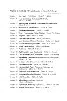
Volume 57 Strong and Ultrastrong Magnetic Fields and Their Applications Editor: F. Herlach Volume 58 Hot-Electron Transport in Semiconductors Editor: L. Reggiani Volume 59 Tunable Lasers Editors: L. F. Mollenauer and J. C. White
Volumes 1-56 are listed on the back inside cover
Electrets Edited by G. M. Sessler With Contributions by M. G. Broadhurst G. T. Davis R. Gerhard-Multhaupt B. Gross S. Mascarenhas G. M. Sessler J. van Turnhout J. E. West Second Enlarged Edition With 227 Figures
Springer-Verlag Berlin Heidelberg GmbH
Professor Dr. Gerhard M. Sessler Fachgebiet Elektroakustik, Universitat Darmstadt, MerckstraBe 25, D-6100 Darmstadt, Fed. Rep. of Germany
Library of Congress Cataloging in Publication Data. Electrets. (Topics in applied physics; v. 33) Includes bibliographies and index. I. Electrets. I. Sessler, G. M. (Gerhard Martin), 1931-. II. Broadhurst, M.G. (Martin Gilbert), 1932-. III. Series. QC585.8.E4E43 1987 537'.24 86-31636 This work is subject to copyright. All rights are reserved, whether the whole or part of the material is concerned, specifically the rights of translation, reprinting, reuse of illustrations, recitation, broadcasting, reproduction on microfilms or in other ways, and storage in data banks. Duplication of this publication or parts thereof is only permitted under the provisions of the German Copyright Law of September 9, 1965, in its version of June 24, 1985, and a copyright fee must always be paid. Violations fall under the prosecution act of the German Copyright Law.
ISBN 978-3-540-17335-9 ISBN 978-3-540-70750-9 (eBook) DOI 10.1007/978-3-540-70750-9 © Springer-Verlag Berlin Heidelberg 1980 and 1987
Ursprilnglich erschienen bei Springer-Verlag Berlin Heidelberg New York 1987. The use of registered names, trademarks, etc. in this publication does not imply, even in the absence of a specific statement, that such names are exempt from the relevant protective laws and regulations and therefore free for general use. 2153/3150-543210
Preface to the Second Edition
The first edition of this volume has been well received by readers and reviewers. In addition to the original English version published in 1980, MIR in Moscow issued a Russian edition in 1983. Since copies of the first edition are now exhausted while interest in the material continues, Springer-Verlag has asked the editor to prepare a new edition. The present second edition contains the seven chapters of the original book and one additional chapter outlining recent progress in the field. The older chapters are essentially unchanged, except for the correction of misprints that came to the attention of the authors. Since the literature on electrets has significantly increased in the interim period, the discussion in the new chapter had to be much more concise than in the existing parts of the book. Even so, many of the new papers could, for reasons of space, not be included. A listing of recent literature concludes the book. The editor expresses his gratitude to his fellow contributors for providing valuable suggestions concerning the new edition and to Springer-Verlag, especially to Dr. H. K. V. Lotsch, for a most gratifying collaboration. Darmstadt, January 1987
Gerhard M. Sessler
Preface to the First Edition
Electrets have, over the past decade, emerged as invaluable components in an ever increasing number of applications. Their usefulness is responsible for the recent impressive growth of research work in a field which had been actively investigated since about 1920. This volume aims to present the fundamental aspects of electret research as well as a detailed review of recent work in this area. The book is broad in scope, extending from the physical principles of the field to isothermal and thermally stimulated processes, radiation effects, piezoelectric and pyroelectric phenomena, bioelectret behavior, and, last, but not least, to applications of electrets. The emphasis of the experimental work discussed is on polymer electrets, but work performed on other organic substances, notably biomaterials, and on inorganic materials, such as ionic crystals or metal oxides, is also reviewed. The interest in polymer electrets is due to the fact that these show extremely good charge-storage capabilities and are available as flexible thin films. In the 1960s attention focussed on highly insulating polymers, such as polytetrafluoroethylene, which have deep traps that store charges for extremely long periods of time. Around 1970, discovery of the strong piezoelectric properties of polyvinylidenefluoride attracted the imagination of many researchers and an enormous amount of work was devoted to the investigation of the physical and chemical properties of this and similar materials. Today, very active research is underway on charge-storage properties of both classes of polymers. The chapters of this book are generally self-contained in the sense that each can be understood on its own. There are, however, many cross-references between chapters which will help to guide the reader to related or supplemental material in other parts of the volume. Uniform symbols and abbreviations are employed for the most-frequently used quantities and polymer names. A list of polymer names will be found in Chapter 1, a partial list of symbols at the end of the volume. Although there have been a few monographs on specific topics of electret research and a number of conference proceedings, a cohesive treatment of the entire field of electrets has so far been lacking. The present volume, by covering many aspects of the field in a relatively small space, is an attempt in this direction. We realize, however, that a number of important questions are not, or not sufficiently, discussed, and that the views held by the different contributors are not always congruent.
VIII
Preface to the First Edition
It is with great pleasure that the editor expresses his gratitude to his fellow contributors, each being a renowned authority in his field, for their collaboration. The preparation and updating of the manuscripts placed a considerable burden on these colleagues, which they carried with understanding. The book is dedicated to Professor Bernhard Gross, himself a contributor, by his fellow contributors. Bernhard Gross is the nestor of electret research, both theoretical and experimental. Apart from this, he has enhanced the knowledge in many other parts of physics. Without his contributions, electret research would not be what it is today. It is with admiration and gratitude that his coauthors devote this book to him.
Darmstadt, September 1979
Gerhard M. Sessler
Contents
1. Introduction
By G. M. Sessler (With 2 Figures) . . . . . . . 1.1 Remarks on the History of Electret Research 1.2 Survey of Physical Properties 1.3 Organization of the Book. References . . . . . . . . .
1
2 6 8 10
2.. Physical Principles of Electrets
By G. M. Sessler (With 28 Figures)
13
2.1 Electric Fields, Forces, and Currents . . . . . 2.1.1 Fields Due to Charge Layers. . . . . . . 2.1.2 Fields Due to Volume-Charge Distributions 2.1.3 Electric Forces . . . . . . . . . . . . . 2.1.4 Currents . . . . . . . . . . . . . . . 2.2 Charging and Polarizing Methods (Forming Methods) 2.2.1 Triboelectricity: Contact Electrification . 2.2.2 Thermal Charging Methods . . . . . . 2.2.3 Isothermal Charge - Deposition Methods 2.2.4 Charging with Liquid Contact . . . . . 2.2.5 Partially Penetrating Electron and Ion Beams 2.2.6 Penetrating Radiation . . . . . 2.2.7 Photoelectret Process. . . . . . 2.3 Methods for Measuring Charge Density 2.3.1 Dissectible Capacitor . 2.3.2 Capacitive Probe . . . 2.3.3 Dynamic Capacitor . . 2.3.4 Compensation Method 2.3.5 Thermal-Pulse Method 2.3.6 Polarization and Depolarization Currents 2.4 Methods for Measuring Charge Distributions 2.4.1 Sectioning and Planing Methods . . . . 2.4.2 Split Faraday Cup . . . . . . . . . . 2.4.3 Combined Induction- Depolarization Method 2.4.4 Light-Radiation Release Method 2.4.5 Thermal-Pulse Method . . . . . . . . . .
13 14
15
17 19 20
22
24 30 32 34 36 37
39 40 40 41 42 42 42 43 43 44 45
46
47
X
Contents
2.4.6 Pressure-Pulse Method . . . . 2.4.7 Charge-Compensation Method . 2.4.8 Indirect Methods . . . . . . . 2.5 Methods for Discriminating between Polarization and Real Charges 2.6 Permanent Dipole Polarization and Real-Charge Storage . 2.6.1 Retention and Decay of Dipole Polarization . . . . . . . 2.6.2 Retention of Real Charges . . . . . . . . . . . . . . . 2.6.3 Spatial Distribution of Dipole Polarization and Real Charges 2.6.4 Analysis ofthe Isothermal Decay of Real Charges 2.6.5 Experimental Results of Real-Charge Decay 2.6.6 Conduction Phenomena . References . . . . . . . . . . . . . . .
48 49 50 50 51 52 54 57 60 66 72 75
3. Thermally Stimulated Discharge of Electrets By J. van Turnhout (With 85 Figures) . 3.1 Introduction . . . . . . . . . 3.2 Mechanisms Responsible for TSD 3.3 Experimental Techniques . . . . 3.4 Methods for Unravelling the Discharge Processes 3.5 Applications ofTSD . . . . . . . . . . . . 3.6 Theory of Current TSD by Dipole Disorientation . 3.6.1 TSD of Dipoles with One Relaxation Time . 3.6.2 Thermally Stimulated Charging of a Polar Sample . ~.6.3 TSD of Dipoles with a Distribution of Relaxation Times 3.6.4 Methods for Distinguishing Between a Distribution in A and in a0 • . • • . . . . . . . . . . • . 3.7 Theory of Current TSD by the Self-Motion of Charges 3.8 Evaluation of TSD Current Data . . . . . . . . 3.8.1 Calculation of Distribution Functions . . . . 3.8.2 Evaluation of Data Pertaining to the Self-Motion of Space Charges . . . . . . . . . . . . . . . . 3.9 Current TSD and Dielectric Measurements . . . . . . . . . 3.10 Current TSD Arising from the Detrapping of Charges . . . . . 3.10.1 Experimental Results of Corona- and Electron-BeamCharged Electrets . . . . . . . . . . . . . . . . 3.11 Some Illustrative Results of Current TSD of Heterocharged Electrets . . . . . . 3.11.1 Inorganic Solids . . . . . . . . . . . 3.11.2 Organic Solids . . . . . . . . . . . . 3.11.3 Organic Solids Incorporated in Clathrates 3.11.4 Supercooled Organic Liquids 3.11.5 Liquid Crystals . . 3.11.6 Biological Materials 3.11.7 Polymers . . . . .
81 83 90 95 99 104 106 106 110 112 116 118 124 127 130 130 135 139 142 143 148 149 150 150 151 153
XI
Contents
3.11.8 Polyvinylidene Fluoride . . . . . . . . . . . . . . 3.11.9 TSD Peaks Arising from the Self-Motion of Space Charges 3.12 Current TSD of Heterogeneous Systems . . . . . . . . . . . 3.12.1 TSD by the Maxwell-Wagner Effect. . . . . . . . . . 3.12.2 Air-Gap Current TSD by Ohmic Conduction and Dipole Disorientation . . . . . . . 3.13 Theory and Practice of Charge TSD. 3.13.1 Some Theoretical Notes. . . 3.13.2 Experimental Results . . . . 3.13.3 Charge Decay Induced by Heat Pulses. 3.14 TSD of Thin Films and Semiconductor Devices 3.14.1 Thermally Stimulated Current Measurements on Semiconductors . . . . . . . . . . . . . . . 3.14.2 Methods Using Thermally Stimulated Admittance and Capacitance . . . . . . . . . . . . . . . 3.14.3 Deep-Level-Transient Spectroscopy. . . . . . 3.15 Analysis of Charge Detrapping by Other Techniques. . 3.15.1 Thermoluminescence and Thermally Stimulated Conductivity . . . . . . . . . . . 3.15.2 Optical Charge Detrapping and TSEE . 3.16 Review of Information Obtainable from TSD . 3.17 Conclusions and Prospects . . . . . . . . . References . . . . . . . . . . . . . . . . . .
161 163 165 165 167 170 171 177 182 184 188 189 190 192 192 196 198 199 201
4. Radiation-Induced Charge Storage and Polarization Effects
By B. Gross (With 30 Figures) . . . . 4.1 Radiation-Induced Conductivity . . 4.1.1 Band-Gap Model . . . . . . 4.1.2 Radiation-Induced Conductivity 4.1.3 Radiation Quantities . . . . . 4.2 General Features of Excess-Charge Transport 4.2.1 Electrode Effects . . . . 4.2.2 The Zero-Field Theorem 4.2.3 Ultimate Charge . . 4.2.4 Carrier Mobilities . . . 4.2.5 Transport Equation 4.2.6 "Floating" Charge Layer 4.2.7 Diffusion . . . . . . . 4.3 Electron Beam Charging . . . 4.3.1 Range-Energy Relations for Electrons 4.3.2 Charge Diagnostics with the Split Faraday Cup 4.3.3 The Threshold Effect . . . . . . . . . . . 4.3.4 The Electron Beam as a Virtual Electrode 4.3.5 Steady-State Currents as a Function of Electron Range 4.3.6 Field- and Charge-Profiles in Irradiated Region . .
. . . . . . . . . . . . . . . . . . . .
217 218 218 219 220 222 222 223 224 225 227 229 229 230 230 233 234 235 236 238
XII
Contents
. 4.4 Charge Diagnostics by Transient Analysis. . . . . . . . 4.4.1 Equivalent Circuit Model and Circuit Equations . . 4.4.2 Short-Circuit Charging and Discharging Currents . 4.4.3 Radiation-Induced Discharge . . . . . . . . 4.4.4 Steady-State Radiation-Induced Conductivity . 4.4.5 Delayed Radiation-Induced Conductivity . . . 4.4.6 Charge Centroid . . . . . . . . . . . . . . 4.4.7 Transit Time Effect and Determination of Mobility . 4.4.8 Breakdown Effects . . . . . . . . . . . . . . 4.4.9 Radiation Hardening and Pressure-Activated Charge Release . 4.4.10 Summary of Electron Beam Data and Methods . 4.5 Gamma-Beam Charging . . . . 4.5.1 Photo-Compton Current . . . . 4.5.2 Space-Charge Formation . . . . 4.5.3 Compton Diodes for Dosimetry . 4.6 Thermally Activated Processes . . . . 4.6.1 Thermally Stimulated Currents and Voltages . 4.6.2 Peak Shift Effects . . . . . . . . . . . . 4.6.3 Positive and Negative Charge Storage by Electron Injection . 4.6.4 Conductivity Glow Curves . . . . . . . . . . 4.6.5 Conductivity Glow Curves for Teflon . . . . . . . 4.6.6 Short-Circuit TSC in a Temperature Gradient . . . . 4.6.7 Radiation-Stimulated Polarization (Radioelectret). . 4.6.8 Polarization Effects in Ionic Solids . . 4. 7 Dosimetry . . . . . . . . . . . . . . . . . 4.7.1 Dosimetry with Self-Biased Systems. . . . 4.7.2 Dosimetry with Externally Biased Systems . References . . . . . . . . . . . . . . . . . .
240 240 242 243 243 244 246 248 250 252 252 253 253 254 256 256 256 258 260 262 266 267 267 269 272 272 274 279
5. Piezo- and Pyroelectric Properties
By M.G. Broadhurst and G. T. Davis (With 18 Figures) 5.1 Thermodynamic Definitions . . . 5.2 Physical Description of an Electret . . . . 5.2.1 Preparation . . . . . . . . . . . 5.2.2 Real Charges- Monopolar Electrets . 5.2.3 Dipolar Electrets . . . . . . 5.3 Symmetry and Tensor Components 5.4 Structure . . . . . . . . 5.4.1 General . . . . . . . 5.4.2 Amorphous Polymers . . 5.4.3 Semicrystalline Polymers 5.5 Properties ofSemicrystalline Polymers 5.5.1 Crystal Relaxations . 5.5.2 Ferroelectricity 5.5.3 Space Charges . . .
285 286 287 287 287 290 294 296 296 296 298 301 301 305 . 308 . . . . . . . . . . . . .
Contents
5.6 Measurements and Data . . . . . . . . . . . 5.7 Dipole Model Applied to Semicrystalline Polymers 5.8 Summary and Conclusions References . . . . . . . . . . . . . . . . . . .
XIII
310 312 315 315
6. Bioelectrets: Electrets in Biomaterials and Biopolymers
By S. Mascarenhas (With 14 Figures). . . . 6.1 Introductory Remarks . . . . . . . 6.2 General Concepts in Electret Research 6.3 Other Dielectric Techniques Complementary to TSDC 6.4 Proteins . . . . . . . . . . . . . . . . 6.5 Bound Water (Structured Water or Biowater) . 6.6 Polysaccharides and Polynucleotides . . . . 6.7 Enzymes . . . . . . . . . . . . . . . . 6.8 Thermally Stimulated Pressure and Bound Water 6.9 Bone, Artificial Biomaterials, and Biomedical Applications 6.10 Natural Electrets. 6.11 Conclusions . References .
321 321 323 329 330 332 334 336 338 340 341 343 344
7. Applications
By G. M. Sessler and J. E. West (With 28 Figures) 7.1 Electret Transducers . . . . . 7.1.1 Microphones . . . . . . . . 7.1.2 Directional Microphones . . . 7.1.3 Headphones and Loudspeakers. 7.1.4 Electromechanical Transducers . 7.1.5 Underwater Transducers 7.2 Electrophotography . . . . . . . . 7.2.1 Xerography . . . . . . . . . 7.2.2 Persistent-Conductivity Methods 7.2.3 Photodielectric Processes 7.3 Electrostatic Recording 7.4 Electret Air Filters . . . . . 7.5 Electret Motors and Generators 7.6 Electret Dosimeters . . . . . 7.7 Piezoelectric Polymer Transducers. 7.7.1 Transducer Principles . . . . 7.7.2 Transducers Using Transverse Piezoelectric Effect 7.7.3 Transducers Using Longitudinal Piezoelectric Effect 7.8 Pyroelectric Polymer Devices 7.8.1 Pyroelectric Response. 7.8.2 Applications. References . . . . . . . . . .
347 348 348 355 358 359 361 362 362 364 364 365 367 368 369 369 370 371 375 376 376 376 378
XIV
Contents
8. Recent Progress in Electret Research
By R. Gerhard-Multhaupt, B. Gross, and G. M. Sessler (With 22 Figures) . . 8.1 Introduction . . . . . . 8.2 Physical Principles . . . . 8.2.1 Charging and Poling 8.2.2 Methods for the Measurement of Charge and Polarization Distributions . . . . . . . . . . . . . . . . 8.2.3 Storage and Decay of Real and Dipolar Charges 8.2.4 Conduction Phenomena . . . . . . . . . 8.3 Thermally Stimulated Discharge of Electrets . . . 8.3.1 Analysis and Refinement of TSD Methods . 8.3.2 Real-Charge Effects . 8.3.3 Dipole Effects . . . . . . . . . 8.4 Radiation Effects . . . . . . . . . . 8.4.1 Conduction and Charge Transport 8.4.2 Irradiation with X-Rays . . . . . 8.4.3 Irradiation with Partially Penetrating Electrons 8.4.4 Analysis of Internal-Field and Space-Charge Distributions by Electron Beams . . . . . . . . . . . 8.4.5 Radiation-Induced Breakdown Effects . . 8.4.6 Dosimetry . . . . . . . . . . . . . 8.5 Piezo-, Pyro-, and Ferroelectric Properties . . 8.5.1 Molecular Conformation, Crystalline Structure and Morphology of Polyvinylidene Fluoride (PVDF) . 8.5.2 Copolymers and Blends (Alloys) with Polyvinylidene Fluoride (PVDF) . . . . . . . . . . . . . . . . 8.5.3 Ferroelectricity and Switching in PVDF and Its Copolymers 8.5.4 Other Piezo-, Pyro- or Ferroelectric Polymers. . . . 8.5.5 Preparation, Modification, and Control of Piezo- and Pyroelectric Electrets . . . . . . . . . . . . . 8.5.6 Theoretical Descriptions of the Piezo-, Pyro-, and Ferroelectricity in Polymer Electrets . 8.6 Bioelectrets . . . . . . . . 8.7 Applications . . . . . . . 8.7.1 Capacitive Transducers. 8.7.2 Air Filters . . . . . . 8.7.3 Piezoelectric Polymer Devices 8.7.4 Pyroelectric Polymer Sensors 8. 7.5 Other Electret Applications References . . . . Partial List of Symbols . . . . Additional References with Titles Subject Index . . . . . . . . . . . .
383 383 383 384 386 388 391 392 393 394 396 399 399 400 401 403 404 405 407 407 408 409 411 411 413 414 415 415 416 417 419 420 420
. 433 . 435 . 443
Contributors
Broadhurst, Martin G. United States Department of Commerce, National Bureau of Standards, Washington DC 20234, USA Davis, G. Thomas United States Department of Commerce, National Bureau of Standards, Washington DC 20234, USA Gerhard-Multhaupt, Reimund Heinrich-Hertz-Institut fiir Nachrichtentechnik Berlin GmbH, Abteilung S+E, Einsteinufer 37, D-1000 Berlin 10, Germany Gross, Bernhard Institute of Physics and Chemistry of Sao Carlos-University of Sao Paulo, Caixa Postal 369, 13560 Sao Carlos, S. P., Brazil Mascarenhas, Sergio Institute of Physics and Chemistry of Sao Carlos-University of Sao Paulo, Caixa Postal 369, 13560 Sao Carlos, S. P., Brazil Sessler, Gerhard M. Fachgebiet Elektroakustik, Universitiit Darmstadt MerckstraBe 25, D-6100 Darmstadt, Fed. Rep. of Germany van Turnhout, Jan Plastics and Rubber Research Institute TNO, PO Box 71, 2600 AB Delft, The Netherlands West, James Edward AT & T Bell Laboratories, 600 Mountain Avenue, Murray Hill, NJ 07974, USA
1. Introduction G. M. Sessler With 2 Figures
An electret is a piece of dielectric material exhibiting a quasi-permanent electrical charge. The term "quasi-permanent" means that the time constants
characteristic for the decay of the charge are much longer than the time periods over which studies are performed with the electret. The electret charge may consist of "real" charges, such as surface-charge layers or space charges; it may be a "true" polarization; or it may be a combination of these. This is shown schematically in Fig. 1.1 for a dielectric plate. While the true polarization is usually a frozen-in alignment of dipoles, the real charges comprise layers of trapped positive and negative carriers, often positioned at or near the two surfaces of the dielectric, respectively. The electret charges may also consist of carriers displaced within molecular or domain structures throughout the solid, resembling a true dipole polarization. If the charges are displaced to domain boundaries they are referred to as Maxwell-Wagner polarization. On metallized electrets, a compensation charge may reside on the electrode, unable to cross the energy barrier between metal and dielectric. Mostly, the net charge on an electret is zero or close to zero and its fields are due to charge separation and not caused by a net charge. An electret not covered by metal electrodes produces an external electrostatic field if its polarization and real charges do not compensate each other everywhere in the dielectric. Such an electret is thus in a sense the electrostatic analogue of a permanent magnet, although electret properties may be caused by dipolar and monopolar charges while magnetic properties are only due to magnetic dipoles. The existence of an external field and the corresponding analogy with a magnet has often been used to define the electret. However, as Heaviside already realized in 1892 [1.1], the fields of an electret may be compensated within a short time period by the relative motion of real charges and dipoles. This is observed in many piezoelectric substances. If one prefers to include some of these materials in the electret category, as Heaviside did, it is necessary to use the broader definition of the electret introduced above based on the permanency of at least one of its charge components and waive the necessity of an external field. However, such a broad definition includes the entire class of piezoelectric substances. We shall in the following adhere to this definition but include from the group of piezoelectric materials only the polymeric substances in the discussions in this book (see also Sect. 1.3). While the classical electrets were made of thick plates of carnauba wax or similar substances, present electret research frequently deals with thin- film
G. M. Sessler
2
SURFACE CHARGES
SPACE CHARGES
DIELECTRIC
~--+---DIPOLAR
CHARGES
(OR DISPLACED)
COMPENSATION CHARGES
Fig. 1.1. Schematic cross section of a one-sided metallized electret having deposited surface charges, injected space charges, aligned dipolar charges (or microscopically displaced charges), and compensation charges
[]D---
-. -
+ + + + + + + + + +
++
(a)
"" +- :!::~
+ + + :;:+ :;:+~ -+ - +.~
(b)
(c)
't-, ;-,:',
(d)
Fig. 1.2a-d. Schematic cross section of some typical electrets without electrodes or with grounded electrodes: (a) nonmetallized monocharge electret, (b) one-sided metallized electret with surface and space charges, (c) one-sided metallized electret with surface charges and charges displaced within domains (Maxwell-Wagner effect) and (d) two-sided metallized electret with dipolar and space charges
polymers such as the Teflon materials polyfluoroethylene propylene (FEP) and polytetrafluoroethylene (PTFE) or polyvinylidene fluoride (PVDF). Typical electrets in present use are 10-50 Jlm thick films of a few cm 2 area, often coated on one or both surfaces with evaporated metal layers. The materials are polarized to charge densities of 10- 8 -10- 6 Ccm- 2 , the charges being trapped real charges in Teflon and predominantly dipolar charges (but additionally trapped charges) in PVDF. In the latter case, the dipolar charges are statically (but not dynamically) compensated by space charges due to conduction in the material. Examples of various nonmetallized and metallized electrets are shown in Fig. 1.2a-d. The charged dielectrics in these figures are either real-charge or dipolar electrets or a combination of these. While the nonmetallized and onesided metallized samples usually exhibit external and internal electric fields, the fields of the two-sided metallized samples are completely contained within the dielectric.
1.1 Remarks on the History of Electret Research Electret properties were already described by Gray in 1732 [1.2] when he mentioned the "perpetual attractive power" of a number of dielectrics, in particular waxes, rosins, and sulphur. He had generated the static electricity of
Introduction
3
these materials by contact electrification caused by cooling of the melts in iron ladles. More than a century later, in 1839, Faraday [1.3] theorized about electret properties due to application of an external electric field when he referred to a "dielectric which retains an electric moment after the externallyapplied field has been reduced to zero". The word "electret" was then coined in 1892 by Heaviside [1.1]. Systematic research into electret properties began in 1919 when the Japanese physicist Eguchi formed electrets from essentially the same materials used by Gray by a thermal method consisting of the application of an electrical field to the cooling melt [1.4, 5]. He found that the dielectrics exhibited charges on their two surfaces which changed sign after a few days from a polarity opposite to one equal to that of the adjacent forming electrode. The charges were later named "heterocharges" and "homocharges", respectively, indicating their relation to the forming electrodes. In the following decades, electrets from wax materials and a number of other substances were produced by charging techniques different from Eguchi's thermal method. One such process, pioneered by Selenyi [1.6] in 1928, depends on the injection of electrons or ions into insulators. Subsequent extension of this work toward development of electrostatic recordings with powders [1.7] and later investigations of photoconductive image formation by Carlson [1.8] culminated in the development of xerography in the 1940s. Related investigations of the effect of light on photoelectric layers by Nadjakoff [1.9] in 1938 remained largely unrecognized. Nadjakoff studied the charge separation occurring in such layers by simultaneous application of light and an electric field, thus discovering the photoelectret. The effect of photoconductivity on internal polarization was later extensively studied by Kallmann and co-workers [1.10, 11] and by Fridkin and Zheludev [1.12]. In the 1950s, a number of charging methods depending on the application of high-energy ionizing radiation were developed. Simplest among these is the bombardment of a dielectric with an electron beam of range smaller than the thickness of the dielectric [1.13, 14]. While Selenyi's work with electron beams was mainly intended for recording, these investigations were performed to study breakdown and thermal charge release. Other similar methods are based on irradiating suitable dielectrics with ionizing radiation, such as penetrating gamma rays or electron beams, and applying an electric field to separate charge carriers generated by the radiation [1.15]. Even without an electric field, charging with gamma irradiation is possible due to Compton currents in the dielectric, as has been shown by Gross [1.16]. During the development of xerography, a simple charging method related to Selenyi's ion-beam technique but depending on the application of a corona discharge was used [1.8, 17] and later extended to thin films [1.18]. Dielectrics were also charged by application of a magnetic field and heat to a dielectric [1.19]. More recently, the charging of thin films with low-energy electron beams [1.20] and liquid contacts [1.21] was reported.
4
G. M. Sessler
While the early period produced a significant amount of experimental data, an understanding of charge storage and charge decay was initially not achieved. The first step toward an explanation of these phenomena was Mikola's observation [1.22] in 1925 that two charges of different nature and of opposite polarity are found on nonmetallized dielectrics charged by application of an external voltage. One of the charges was assumed to be an internal polarization caused by ionic displacement while the other charge was ascribed to a deposition of ions onto the surfaces. Adams [1.23] in 1927, in an attempt to explain the charge decay theoretically, postulated again the presence of two charges, both being due to internal phenomena. These were assumed to be a volume polarization and a "compensating" charge at the surface, the latter being induced by the field of the former. The charge reversal and eventual decay was then explained as being due to the slow decay of the volume polarization and the time lag in the corresponding decay of the compensating charge. Further investigations were made by Gemant [1.24] in 1935 who confirmed the polarity reversals found by Eguchi and introduced the terms "heterocharge" for a charge of polarity opposite to that of the adjacent forming electrode and "homocharge" for a charge of equal sign. Convincing evidence for the presence of two different types of charge and identification of these charges was eventually offered in a series of fundamental studies by Gross [1.25, 26] in the 1940s. He extended the experimental knowledge by measurements of polarization and depolarization currents and charges at varying temperatures and by sectioning experiments. It was demonstrated that the heterocharge is linked to dielectric absorption involving dipoles in polar substances or ionic charges in other materials while the homocharge is due to interfacial charging between electrode and dielectric. Gross also derived many of the fundamental relationships governing the fields and charges in a dielectric and the adjacent air gaps and electrodes. The twocharge theory was subsequently used by Swann [1.27] as the basis of a phenomenological theory of open-circuit charge decay, extended later on by Gubkin [1.28] to short-circuit conditions. In 1937, Gross [1.29] first used the Boltzmann-Hopkinson superposition principle, valid for linear dielectrics, to develop a mathematical formalism for the discharge of electrode charges over the internal resistance of the dielectric and for the decay of a polarization in the dielectric. Later, Wiseman and Feaster [1.30] obtained further extensive confirmation of the validity of this principle by demonstrating that the response of a dielectric to a series of polarization steps is a linear superposition of the individual responses. Perlman and Meunier [1.31] then applied the principle to the open-circuit decay of unshielded dielectrics and thus explained the charge decay in carnauba wax. Further insight into the nature of charge retention was achieved from the studies of Gerson and Rohrbaugh [1.32] which indicated that carrier trapping could play an important role in electrets. Dramatic progress was made by the introduction of the thermal depolarization method, first used by Randall and Wilkins [1.33] for the in-
Introduction
5
vestigation of phosphorescence, into electret research. In 1964, this method was applied to the case of dipole polarization by Bucci and co-workers [1.34, 35] who suggested the name ionic thermal conductivity (lTC). It allows determination of the activation energy and dipolar relaxation time from a measurement of the depolarization currents obtained upon linear heating of the dielectric. A host of recent work has been devoted to the application of lTC methods or related thermally stimulated current techniques for investigating dipolar and space-charge phenomena respectively [1.36-41]. These studies have culminated in a very comprehensive treatment by van Turnhout [1.42]. Of similar importance are recent studies of isothermal charge transport in insulators, taking into consideration the effect of trapping on excess-charge currents [1.43-49]. This work has also been extended to irradiated materials [1.50] and materials with non-uniform conductivity [1.46]. Additional information has been gainel from de and ac conductivity measurements on poorly conducting materials and from the interpretation of such data [1.47, 48, 51, 52]. Recently, charge transport in amorphous solids has been discussed in terms of a stochastic transport model [1.53]. This model describes the dynamics of a group of carriers executing hopping processes in an electric field with a wide distribution of hopping times. Such analyses with and without consideration of trapping phenomena yield a number of important conclusions about charge transport. Much of the newer experimental work was done on polymer electrets which, although chemically not as well defined as many inorganic materials, have gained importance due to their usefulness in practical applications. Piezoelectric properties of biological and polymeric materials were already investigated by Fukada and others in the 1950s and 1960s [1.54]. Of particular importance was the discovery by Kawai in 1969 of a strong piezoelectric effect in the polymer PVDF [1.55]. Due to a host of actual and potential applications of piezoelectric polymer materials, this subject has now developed into a very active area of research [1.56--60]. Apart from the use of charge-storage phenomena in xerography and a few other areas, where extreme permanence of the polarization is not required, applications of electrets came only recently. Actually, long-lived electrets were generally considered a scientific curiosity until the late 1960s when, a few years after the description of the first polymer-film electret microphone in 1962 [1.61], such transducers were introduced commerically on a large scale. Presently, work on the use of electrets in dosimeters, transducers, pyroelectric detectors, prosthetic and switching devices, gas filters and other instruments is being performed by a number of laboratories [1.62-67] and a series of commercial applications have been reported (see Chap. 7). This has stimulated a considerable increase in very recent electret research. The early literature on electrets was reviewed by several authors (e.g., [1.68, 69]), notably by Fridkin and Zheludev [1.12] and Gross [1.70], while the more recent work is discussed in a number of articles of different scope (e.g.,
6
G. M. Sessler
[1.71, 72]), in the proceedings of several conferences [1.73-75], and in van Turnhout's monograph on thermally stimulated currents [1.42].
1.2 Survey of Physical Properties Physical properties of particular interest in electret research are conductivity, mobility, dipolar relaxation frequency, and piezo- and pyroelectric constants. To explain the differences between various classes of electrets, and distinguish them from other dielectrics, a brief discussion of these properties is necessary. If a dielectric has mobile intrinsic charge carriers, it exhibits an intrinsic conductivity g. This conductivity is responsible for the decay of excess real charges within the material. In the simplest case, if the excess charges are located on the surfaces of an open-circuited sample (e.g., a nonmetallized dielectric) and decay through the dielectric without giving rise to space-charge effects, the time constant T of the decay is given by T 1 =aa0 jg. Even in nonconductive materials (devoid of intrinsic carriers), an excess charge decays due to the carrier mobility. A charge located initially on the nonmetallized surface of a one-sided metallized sample of thickness s spreads under its field through the dielectric within the so-called transit time given by t 0 ;. =s 2 jpV0 , where pis the mobility and V0 the initial voltage generated across the sample by the charge. The mobility may be affected by trapping events. The decay of a uniform dipole alignment is, in the simplest case of a single dipole relaxation frequency and in the absence of an internal field (i.e., for a short-circuited dielectric), determined by a relaxation time T 2 = 1/o:. Mostly, an entire spectrum of relaxation frequencies is present. Piezoelectric properties are found in noncentrosymmetrical crystals which account for 21 of the 32 crystal classes. Ten of these belong to the polar classes and are also pyroelectric. Piezoelectricity (and in some cases pyroelectricity) occurs in single crystals (such as quartz), in polycrystalline materials (such as PZT), and in materials with crystalline and amorphous regions (such as PVDF). While piezoelectric crystals show spontaneous polarization, the polycrystalline or partially crystalline materials have to be poled at an elevated temperature by application of an electric field. Piezo- and pyroelectric effects can also occur in space-charged dielectrics, but only in cases where either a mechanical anisotropy (e.g., due to a domain structure or to stiff electrodes deposited on the material) or inhomogeneous strain is present [1.76]. Whether this yields a sizeable contribution to the observed piezo- and pyroelectric effects remains in question [1.57, 77]. Some piezoelectric polymers show also cooperative interactions within groups of molecules and thus resemble ferroelectric materials. Evidence of cooperative phenomena is, for example, found in the poling hysteresis ofPVDF [1.60]. X-ray diffraction studies on PVDF also give results consistent with the assumption that the material is ferroelectric [1. 78]. Typical properties of some electret materials (including piezoelectric substances) are shown in Table 1.1. The piezoelectric materials are all characterized by a very slow dipolar relaxation. Due to their relatively high conductivity,
crystalline or polycrystalline
crystalline and amorphous regions
Anthracene Naphthalene
PVDF
Quartz
PZT-5
Photoelectret
Piezoelectric polymer
Piezoelectric crystal
Piezoelectric ceramic
polycrystalline
crystalline
2 X 10 2 102
> 10 2
> 10 3
10 -,sd 10-14e
< a::
10-4
10
10 2
ELECTRON ENERGY (keV)
Fig. 2.9. Practical or extrapolated electron range for aluminum; PTFE, FEP (Teflon); PET (Mylar); and PP (polypropylene); (the data for the polymers are derived from the aluminum range by dividing through the density ratio)
range, which is about 2/3 of the practical range shown in Fig. 2.9. Depending upon the field direction, additional charge motion takes place. In one-sided metallized samples the field is essentially directed toward the electrode (a small field toward the positive surface layer also exists). Thus, most electrons penetrate beyond the average range into regions where the RIC is still large enough to allow inward motion of electrons or outward motion of holes. This process is completed within minutes after termination of charging (see also Sect. 3.13). More details of the charge-penetration process will be discussed in Sect. 2.6.3. For Teflon, the resulting charge arrangement is stable over periods of the order of tens of years at room temperature [2.62]. Practical implementations of electron-beam setups use glow cathodes or rf discharges for electron generation, electrostatic beam focusing, and an acceleration voltage of 5-50 kV. To ensure a uniform current density over the irradiated cross section, scanned beams are occasionally used [2.59, 63, 64]. Alternatively, scanning electron microscopes have been employed as electron beam sources. Because of their beam uniformity, such instruments can be used in the static or scanned mode. In the target chamber dielectric samples, generally metallized on the rear surface, are exposed to the electron beam for periods of 1 ms up to a few s by opening and closing a mechanical shutter. During exposure the current to the rear electrode, corresponding in magnitude to the net injection current, is monitored. Thus the dielectric can be charged to a predetermined value. The method has also been adapted to charging long strips of foil utilizing a roller arrangement [2.64]. The stored charge has great lateral uniformity if the electron beam is uniform. Measurements of the lateral charge distribution on typical electronbeam charged samples show non uniformities of less than ± 5% which are probably due to spurious charges present on the dielectric before irradiation.
36
G. M. Sessler
Ion-beam injection, having the above-mentioned drawback, is not widely used. However, charging of selenium by bombardment with a variety of 5-400 eV ion species [2.47] has demonstrated the feasibility of this technique. The advantages of electron-beam charging are the complete control over charge depth, lateral charge distribution, and charge density possible with this method. These features have made electron-beam injection an important tool for the charging of electrets used in research and for the study of solid-state properties relating to charge trapping and charge decay [2.29, 59, 61, 62, 64, 65]. In addition, electron-beam charging is now being used extensively for charging membranes of electret microphones.
2.2.6 Penetrating Radiation
Dielectrics can be charged by internal displacement of carriers generated by various kinds of completely penetrating radiation. The carrier displacement may be accomplished by externally applied or internal fields. A number of experiments with y rays, X-rays, f3 rays, and monoenergetic electron beams were performed along these lines yielding electrets which are generally less stable than those produced by other methods (see below). Correspondingly, most of these studies were motivated by an interest in the effect of radiation on various properties of solids (related, among others, to radiation dosimetry) rather than by the desire to produce stable electrets [2.66]. A brief account of these methods will be given here and further discussion deferred to Chap. 4. In the classical charging processes of this kind the dielectric, with a voltage applied across its thickness, is subjected to penetrating radiation from a particle accelerator, an X-ray machine or a radioactive source. After exposure to a total dose of 1-106 rads, the radiation is terminated and the voltage removed. The sample now exhibits electret properties and is often called a "radioelectret." The charging has been explained in terms of molecular ionization followed by carrier drift and carrier trapping [2.67]. The irradiation produces electron-hole pairs which drift in the applied field toward the electrodes, resulting in charge separation. Eventually, the carriers are trapped, giving the dielectric a heterocharge. More recently, thermoluminescent materials such as LiF and CaF 2 have been charged by similar methods [2.68, 69]. In these experiments, relatively small doses (1-10 3 rads) of X-rays are used to irradiate samples subject to external or internal electrical fields, the latter being due to prior thermoelectret polarization. The irradiation generates again secondary electrons and holes which are trapped, forming a space-charge distribution detectable in thermally stimulated current experiments. In CaF 2 the charge generated per rad of irradiation is five orders of magnitude greater than in Teflon-disk radioelectrets and about one order of magnitude greater than in Teflon film electrets [2.70]. The effect is thus of interest in radiation dosimetry (see Sect. 4.7).
Physical Principles of Electrets
37
Charging of dielectrics with penetrating radiation is also possible in the absence of an applied electric field. One such method depends on the use of
Compton electrons produced by high-energy X-rays and y rays [2.71]. These electrons are scattered preferentially in the forward direction and thus give rise to a space-charge polarization of the dielectric. Since the angular distribution of the scattered electrons becomes increasingly isotropic with decreasing energy, the effect is more pronounced at higher energies of the primary photon radiation (around 1 MeV). Thus, rather thick layers are needed for optimal polarization. Another method not requiring an applied field utilizes an electron beam that penetrates the sample to be charged before being absorbed by a backup insulator. Due to the charge buildup in the insulator and the related electrical fields, electrons drift from the insulator to the sample (possibly by spark discharges in the gap) causing a charging effect [2.72]. The method has been used for the charging of polymer-film electrets. All charging methods depending on penetrating radiation generate a radiation-induced conductivity throughout the dielectric which decays slowly after irradiation [2.61]. Electrets produced by such methods are therefore inherently less stable than electrets charged by other methods. However, as has been pointed out above, the charging effects due to penetrating radiation can be utilized in radiation dosimetry. 2.2. 7 Photoelectret Process
The photoelectret process depends on the use of light rather than high-energy radiation but is otherwise very similar to the above radioelectret procedure. The materials, generally photoconductors, are coated with one or two transparent electrodes and irradiated with ultraviolet or visible light under an applied field. After termination of the irradiation and removal of the field, a permanent polarization (often referred to as "persistent internal polarization") is found in the dielectric, now called a "photoelectret". The classical experiments on ZnCdS, phosphors, anthracene, etc., have been thoroughly reviewed in the literature [2.25, 73]. More recently, photoelectret charging was also performed on thin films of cadmium sulfide [2.74] and on amorphous semiconductors [2.75]. The "polarization" is attributed to carrier generation by the light, displacement by the applied field, and eventual trapping; dipole polarization has been ruled out [2.73, 76]. The carrier generation can be readily caused by light of wavelengths shorter than the absorption edge of the photoconductor. The displacement of carriers due to the applied field is dependent upon the carrier mobilities in the bulk of the material as well as the height of the dielectric-electrode barrier. If the bulk mobilities of both carrier types are large and the barriers are high for at least one type of carrier, charges will accumulate at one or both dielectric-electrode interfaces. One obtains a "barrier polariza-
38
;
..
~ 4
~ >
G. M. Sessler
90
80 70
0
...
0 0 0: 1-
...u ...J
UJ 0 UJ
1-
"-
:J
2
4
6
a
POLARIZING TIME
10
12
(minutes)
14
16
Fig. 2.10. Photoelectric polarization in anthracene as function of polarizing time for various ultraviolet intensities: (a) 2.2 x 10- 8 W Cm- 2 ;(b)4x 10- 9 W cm- 2 ;(c)7J X 10- 10 Wcm- 2 ;(d)1.3xl0- 10 Wcm- 2 ;(e)l.4x 10- 11 W em - l (polarizing voltage ~ 300 V)
tion". If, however, the mobilities are such that only one carrier type is significantly displaced, or if the irradiation is nonuniform over the thickness of the sample, "bulk polarization" is produced. This case can obviously occur irrespective of the barrier heights. Trapping, detrapping, and retrapping may occur during irradiation; after irradiation, the charge distribution is greatly immobilized, but still subject to a dark decay (typically over periods of the order of days). Results demonstrating the effect of polarizing time and light intensity on the electret charge of anthracene are shown in Fig. 2.10 [2.76]. The figure indicates that for very low intensities the charge increases almost linearly with time but appears to saturate at higher intensities. Other experiments yielded a time dependence given by an expression of the form of (2.56), where the time constant r relates to light intensity while, for a given material, crm is only a function of voltage (generally proportional to voltage). This means that the curves in Fig. 2.10, obtained for the same polarizing voltage, will eventually all reach the same saturation charge. It was also shown that the charge is a weak (logarithmic) function of the light intensity. Certain materials show a considerable "dark polarizability" (the ability to produce a polarization by field alone) if preirradiated in the absence of a field. This dark polarizability decreases more slowly with time than the dark decay mentioned above [2.73]. Such different behavior has been attributed to the fact that the dark decay occurs due to drift under the internal field while the dark polarizability decreases because of the recombination of radiation-produced positive and negative carriers in the field-free sample. The second process, taking place in the absence of a field, is slower than the first. Similar differences in field-dominated and field-free decays were recently found in gammairradiated Teflon samples [2.70].
Physical Principles of Electrets
39
The photoelectret process is of little practical use as a charging method. The reverse effect, however, namely the discharge of a polarization on photoconductors (particularly selenium) by irradiation with light is of great practical importance in xerography. In this application, the charging is achieved by a corona process (for details on xerography see Chap. 7).
2.3 Methods for Measuring Charge Density A measurement of the net charge
s
a= Jg(x)dx 0
[see (2.19)] in a dielectric can
easily be performed by dropping the dielectric into a Faraday cup (a metal container) and measuring the induction charge flowing from ground into the cup. It follows from simple electrostatics that this induction charge is opposite in sign but otherwise equal to the net charge in the dielectric. In most cases, however, one is more interested in determining the moment of a charge distribution rather than the often small (or vanishing) net charge. For nonmetallized or one-sided metallized electrets, this can be achieved by measuring the induction charge on a planar electrode parallel to the electret surface. As has been shown in (2.24), the induction charge ail generated by an electret backed up by a metal plate is proportional to the projected or effective surface-charge density a1 . For a contacting electrode, ail actually equals -a 1 . As has been further demonstrated, a surface charge 8' 1 generates the same external field as the actual charge distribution g(x). Thus 8' 1 is the only quantity that can be determined by a single induction measurement. In spite of the limited information obtainable from induction measurements, such methods are widely used because of their simplicity. They will be discussed in Sects. 2.3.1-4 (see also reviews in [2.77, 78]). In Sect. 2.3.5 a method to determine the total charge 8' will be reviewed. This method consists of two separate measurements. Data on charge density of two-sided metallized electrets can be obtained in certain cases from measurements of polarization or depolarization currents, as shall be shown in Sect. 2.3.6. Methods for determining the polarization charge of piezoelectric electrets are based upon the actual evaluation of the piezoelectric and pyroelectric properties [2. 79-81]. Other techniques of measuring charge density, depending on the deflection of particle beams [2.82, 83] and the force exerted on electrodes (ponderomotive meters [2.77, 84]) are less convenient to instrument than the purely electrical procedures and often affect the charges to be measured. They are therefore not widely used. Optical methods based on a measurement of birefringence or the amount of second-harmonic generation have also been described [2.85, 86]. For a discussion of these methods, the reader is referred to the literature.
G. M. Sessler
40
2.3.1 Dissectible Capacitor
The dissectible capacitor, going back to Benjamin Franklin (see [2.87]), is the classical method of determining the effective surface-charge density on dielectrics. In its simplest implementation, it consists of two electrode plates connected by a ballistic galvanometer or by a capacitively shunted electrometer. The charged dielectric is placed between, and in contact with, the electrodes generating induction charges on them. If one of the electrodes is lifted from the dielectric, its induction charges will flow into the galvanometer or capacitor. They can be measured if the time constant of the galvanometer or that of the capacitor-electrometer combination is much larger than the time required to remove the electrode. Due to possible air gaps between the electrodes and the dielectric, the induced charge O"il on the electrode may be smaller than the effective surfacecharge density 8" 1 on the electret. The relation between O"i 1 and 8" 1 for a onesided metallized electret has been given in (2.24). For plate electrets, stfs is generally small so that O"i 1 equals - 8" 1 . For thin-film electrets, however, s 1 and s are often comparable, and s 1 has to be accurately determined, e.g., from a capacitance measurement. The dissectible-capacitor method requires only simple instrumentation. Its drawbacks are the occurrence of contact electrification and breakdown in the air gap, affecting the measurement of small and large charge densities, respectively. A further problem with the study of thin-film electrets is the effect of the air gaps discussed above and their nonuniformity. These drawbacks have largely eliminated dissectible-capacitor methods in modern electret research. 2.3.2 Capacitive Probe
The capacitive probe is related to the dissectible capacitor but avoids its drawbacks by using a well-defined and relatively large air gap of thickness s 1 between probe and electret [2.77, 88-91]. If the probe, which may be stationary, is exposed to the field of the electret, a charge aO"il flows into it from a parallel capacitance C. This charge is given by aO"il = - CV, where V is the voltage generated across C. As long as C is much larger than the capacitance of the probe, O"il equals the short-circuit induction charge and one has therefore for a one-sided metallized electret from (2.24)
'-(1 +Sl&)CV -a '
(T-
1
SB 1
(2.59)
where all the quantities on the right are accurately measurable.
A schematic view of such a setup is given in Fig. 2.11. For measurements on thin-film electrets the probe is typically a few mm above the electret surface permitting charge-density measurements up to 10- 6 C·cm- 2 . Use of a shutter
Physical Principles of Electrets
41
ELECTROMETER
Fig. 2.1 t. Schematic drawing of a capacitive-probe setup for measuring projected-charge densities. C =external capacitor, R =input resistance of electrometer, S =switch. [2.91]
allows one to shield the probe from, and later expose it to, the field of the electret. The voltage across C is then measured with an electrometer (input resistance R) and the charge density determined with (2.59) within a time much less than r = RC. Calibration of such a setup is possible by replacing the electret by a two-sided metallized sample of equal thickness whose top surface is charged to a known voltage. Various probe sizes yield different resolutions, while a micropositioner allows use of the instrument as a "local-charge meter" for mapping charge distributions. Fully automatic local charge meters of similar design have also been described [2.77]. Advantages of capacitive-probe methods are the great accurancy typical for static techniques with well-defined geometry and the noncontacting measuring procedure. Such methods can be easily used to determine average charge density as well as lateral charge distribution. The measuring range extends from 5x 10- 11 to above 10- 6 C·cm- 2 . 2.3.3 Dynamic Capacitor
The dynamic-capacitor method utilizes a measurement of the ac voltage induced on an electrode near an electret [2.92]. The voltage is due to field variations which are either caused by mechanical excitation of the electrode (or the electret) or by periodic shielding of the electrode by a rotating shutter. In all cases, the relation between charge density and generated voltage depends on circuit details and will not be given here. The measuring accuracy may be improved by filtering, amplifying, and automatically registering the generated ac voltage. As compared to the capacitive probe, the dynamic-capacitor method is mechanically somewhat more complicated and not as easy to use. On the other hand, it allows the application of signal-processing techniques and the perfor" mance of measurements with small probes at operating frequencies w sufficiently high so that RC ~ 1/w holds for the RC constant of the circuit.
42
G. M. Sessler
2.3.4 Compensation Method Like the dynamic capacitor, this method depends on vibrating the electret or the opposing electrode. However, instead of measuring the induced ac voltage, one compensates the field of the electret in the air gap with a de voltage V0 until the ac voltage (and thus the field E 1 ) vanishes [2.29, 35, 93, 94]. The effective surface-charge density for a one-sided metallized electret then follows from (2.22) with E 1 =0 and s 2 =0 as (2.60)
This method is also a noncontacting procedure. It has the additional advantage that a measurement of the air-gap thickness is not necessary to determine iJ 1 . Highly automated setups of this kind have been developed in several laboratories [2.29, 95].
2.3.5 Thermal-Pulse Method An elegant method to determine the total net charge stored in one-sided metalized electrets is the thermal-pulse technique, which is in wide use for the study of charge centroids (for details of this method, see Sect. 2.4.5). If the centroid location r of the charge distribution is determined with this method, the total charge follows from ,
ee 0 V
(J=-_-,
r
where V is the surface potential of the electret. Thus, measurements of V and r have to be performed.
2.3.6 Polarization and Depolarization Currents The induction methods discussed in Sects. 2.3.1-5 can only be used on samples having at least one nonmetallized surface. On samples metallized 'on both surfaces charge densities may be determined in certain cases by measuring the polarization or depolarization currents from the two electrodes. One example is real-charge injection, e.g., by electron-beam charging with a partially penetrating beam. In this case the injected charge is equal in magnitude to the integral over the compensation current into the nonirradiated (rear) electrode if the front electrode is floating. Another example is the decay of a uniform volume polarization. Since every polarization charge in the dielectric induces an image charge on the electrode, the polarization is equal in magnitude to the integral over the externally measured polarization (or depolarization) current [2.8].
Physical Principles of Electrets
43
The situation is more complicated for real-charge release within the dielectric, where drift of charges to the electrodes generally does not release an equal number of image charges. According to (2.20) and (2.25) the image charge induced on a contacting electrode changes very little if a space charge initially trapped close to an electrode drifts to this electrode. For example, a charge layer of density a 0 at a depth x 0 in the dielectric releases a charge a 0 x 0 /s from the far electrode if the drifts are unidirectional and less if they are bidirectional. Since the latter predominates for deep charge layers in homogeneous dielectrics, the released charge is actually always less than 15% of the stored charge [2.29]. However, in electrets with regions of relatively high conductivity, such as samples charged by injection methods, drifts may be unidirectional and the amount of released charge can approach the amount of stored charge. An example is an electret in which carriers injected through one surface and trapped close to the other surface generate a high radiation-induced conductivity throughout the penetrated volume. Upon depolarization, the carriers drift to the surface of injection, thus releasing a large electrode charge. In cases of unidirectional drift (near-surface charge or conductive region) measurement of the charge released by depolarization will therefore give information about the density of the stored charge if its average depth is known.
2.4 Methods for Measuring Charge Distributions Sectioning methods and potential probe techniques are the classical procedures of measuring the distribution of polarization charges and real charges [2.96, 97]. Sectioning techniques in particular have been used extensively on thick electrets and have yielded a wealth of information. Because oflimitations of the slicing procedures, these methods are of little use for thin-film electrets. For such dielectrics, techniques depending on the measurement of charging and charge-release currents or on the evaluation of voltage changes due to heat, ultrasonic, or optical excitation have been developed. These methods yield the centroid location (mean depth) of the charge distribution or even the actual distribution in the thickness direction of the electret.
2.4.1 Sectioning and Planing Methods On electrets of sufficient thickness, sectioning and planing methods permit the measurement of the distribution of polarization and real charges. Such experiments have been originally performed on wax electrets which are soft enough to allow cutting and shaving operations, but have been extended more recently to polymer electrets. Typically, the electret is divided into a number of thin disks by cutting along planes perpendicular to the direction of polarization. To avoid loss of charge, the cutting is performed at low temperatures. Also, care has to be
G. M. Sessler
44
taken to prevent contact charging due to the cutting. The sections may now be studied by charge and depolarization-current measurements. The net charge of an electret section of thickness s' can be determined by putting the slice into a Faraday cup. Since polarization charges (dipoles and microscopically displaced charges) have zero net charge, this experiment s'
determines the net real charge, 6-r = f Qr(x)dx. If these charges are of one polarity 0
within the section, as is to be expected for s' ~ s, 6-r equals the total real charge. A measurement of the short-circuit depolarization current of a thin electret section having a uniform polarization P p(t) and a uniform real charge Qr(t) yields the polarization PP [2.98]. This is seen by substituting (2.20) with (2.3) and (2.5) into (2.42). One obtains (2.61) Integration over time yields the charge released over the electret area a, CIJ
Q
00
=
aPP(O)- !as' Qr(O) +a
f iJO, t)dt.
(2.62)
0
On thick sections, Q 00 includes polarization and space-charge contributions. However, with decreasing s', the second term on the right goes to zero. The same is true for the third term since ic is proportional to E(O, t) [see (2.37)] which decreases with decreasing real charge within the section. Progressively thinner slices of an electret will therefore give a depolarization current which tends toward a thickness-independent value determined only by the polarization P p· Measurements on such sections thus yield the polarization charge of an electret. Alternatively, planing experiments can be performed by shaving thin layers off the dielectric and measuring either the charge on the shaved-off sections or the charge on the remainder of the sample [2.99]. Present slicing techniques permit the removal of layers down to about 5 11m thickness [2.100]. This determines the current resolution of the sectioning method.
2.4.2 Split Faraday Cup
The split Faraday cup method [2.61, 101] allows one to determine the centroid location of real charges for a two-sided metallized electret charged by electron injection. Measurements of the induction charges on the two electrodes ("split Faraday cup") during and immediately after charging are required. The spatial depth on electrets with only one electrode can also be determined by a
Physical Principles of Electrets
45
modification of this method. These procedures yield accurate results only if dipole or other volume polarizations are absent. The method is illustrated in Fig. 4.16 and discussed in Sect. 4.4.6. Briefly, the dielectric is irradiated with floating front electrode (open circuit) and a buildup of the induction charge on the rear electrode is measured. Thereafter, the irradiation is terminated and the front electrode connected to ground. The induction charges are now distributed between front and rear electrodes and have the values Q1 and Q2 , respectively. Measurement of these quantities allows determination of the mean charge depth r by means of [2.61] (2.63) Often, the spatial depth changes with time after short circuit. This change can also be detected from the time dependence of Q1 and Q2 • On samples metallized on the rear side only, a measurement of the rearelectrode charge Qm at the end of beam charging and of the charge Qi induced on a contacting front electrode after charging yields the mean depth [2.62] (2.64) The Faraday-cup method depends on measurements taken during the charging of the electret. If such measurements are not available, the combined induction-depolarization method or the thermal-pulse method can be used. A method developed for Townsend discharge electrets utilizes bridge measurements to determine the charge density on the sample and the potential difference across it. These measurements also allow one to determine the spacecharge depth [2.55, 102].
2.4.3 Combined Induction-Depolarization Method
The centroid location of real charges on previously charged electrets can be determined by a method utilizing an induction-charge measurement and a measurement of the integrated depolarization current [2.103]. It is applicable to nonmetallized or one-sided metallized electrets with either a single-polarity charge distribution or a distribution consisting of a positive and a negative cloud of charges. Dipole or other volume polarizations are to be absent. The first step of the procedure consists of a measurement of the effective surface-charge density a 1 on the top (nonmetallized) surface by an appropriate method (see Sect. 2.3). Thereafter, a complete depolarization of the sample by application of heat, radiation, light, or other means is performed while the co
integral over the depolarization-current density q co =
Ji · dt through contacting 0
electrodes is determined. For a single-polarity distribution, the mean charge
G. M. Sessler
46
depth i', measured from one of the electret surfaces, is then given by (2.65) where the assumption is made that all charges drift to that surface (see below). For a distribution consisting of positive and negative charge clouds, the expression on the right-hand side of (2.65) can also be used to measure charge depth if all the positive carriers drift to one surface while all the negative carriers drift to the other surface. In this case, r is the sum of the mean positive and negative drift distances. Under the same conditions, the total trapped charge in the dielectric can be determined from s
Jlgr(x)ldx=lqooi+ICJll.
(2.66)
0
The requirement of unidirectional drift for carriers of one polarity is approximately met in a number of cases of which two are particularly important. Such drifts are always encountered if the charges are stored close to one surface (approximately within 20% of the sample thickness) and if retrapping of the carriers is fast [2.29, 103]. These conditions are met in some polymer materials, such as Teflon, surface-charged with thermal, liquidcontact, or other methods. Unidirectional drifts occur also in electrets charged to any depth with electron-beam methods. In this case the drift is back to the surface of incidence through the volume modified by the radiation-induced conductivity. This holds even for samples where the electrons have been injected to a depth beyond the center. 2.4.4 Light-Radiation-Release Method
The centroid location of charges in photoconducting electrets metallized on both surfaces with semitransparent electrodes can be determined by a lightradiation-release method [2.104]. The sample is first irradiated through one of its electrodes with light that is sufficiently absorbed so that it does not penetrate beyond the charge layer. Due to detrapping of the stored charge Ql' or drift of secondary carriers generated by the light, the stored charge is completely neutralized. Thus, an external charge QA equalling Qt(s- f)/s, where r is the depth measured from the nonirradiated surface, is released. A similar experiment (on a different portion of the sample) performed with irradiation through the other electrode yields a released charge Q8 = Ql/s. From these relations, i'/s can be determined as (2.67)
Physical Principles of Electrets
l llll LIGHT
THIN METAL COATING
PULSE
47
12~----------------------------~
TENSIONED ELECTRET FOIL
v 0
AIR GAP
SENSING ELECTRODE ~~-------~
1 X
[\]
GUARD RING
TO RECORDING APPARATUS
Fig. 2.12. Experimental setup for mea· suring charge distribution in x-direction by thermal-pulse method [2.106]
Given charge distribution:
..
!! c
·c:; 1
.
;;:
't 0
u
\llflll
~
a
" u.
6
·~ 0
u
~
ti ~
numerical limit
4
"· .........
@close to metalized side
0
in the center of the foil @close to nonmetalized side
.....·'b-·+·--1.·-·l!r-·+·-·-·-
·-fl....~llll
,.
I I
I
0 ~,~: lii 'x, ,, X .c 2 E ', ""K-x--x--oo«-- -x-- -x- ----«--oo«--z" Relative difference in voltage response (%)
Fig. 2.13. Number of Fourier coefficients of charge distribution that can be determined with an accuracy of 20% or better as function of the accuracy to which the voltage response in a thermal-pulse experiment is measured [2.108]. Each symbol represents a charge distribution
The main features of the charge distribution in a relatively thick electret can also be determined by an optical method. The distribution follows from the charge released by irradiation with a light beam propagating through the sample normal to the direction of polarization [2.105]. 2.4.5 Thermal-Pulse Method
The centroid location of real and polarization charges in electrets can also be determined from measurements of the potential change across the dielectric upon absorption of a light pulse by the sample surface and diffusion of the corresponding heat into the sample [2.106]. A schematic illustration of the method is given in Fig. 2.12. The potential of the nonmetallized surface of a one-sided metallized electret relative to the electrode is by virtue of (2.30) V =siT 1 /ee 0 . As the heat diffuses through the dielectric, changes in sand iT 1 due to thermal expansion and changes in B cause corresponding changes L1 V of V. If measurements of L1 V are taken at time t 1 when the thermal pulse has just entered the electret and at time t 2 when it is uniformly distributed over the dielectric, one has (2.68) Thus, a measurement of the voltage transient allows one to determine r. Experiments of this kind are nondestructive since the thermal pulse results only in a minor temperature increase of the sample.
48
G. M. Sessler
It has also been suggested to use this method to detect more details of the spatial distribution of the charge [2.106]. Since the voltage change at time t as function of the temperature increase AT(x', t) is, for a real charge, given by
l
AV(t)cx: [Q.(x)I AT(x', t)dx'] dx
(2.69)
it appears possible to calculate (lr(x) by deconvolution of the integral if AT is known. Yet, because of inaccuracies of the deconvolution procedure, a unique solution for Qr(x) is generally not obtained. All that can be determined under ideal conditions are 5-10 spatial Fourier coefficients of the distribution [2.107, 108]. However, if one has to allow for measuring errors in the voltage response, even fewer coefficients are accurately found. This is shown in Fig. 2.13, where the number of Fourier coefficients determined to better than 20% is given as a function of the accuracy to which A V(t) is measured [2.108]. The figure indicates that for a measuring accuracy of 0.1 %, only 3-9 coefficients, the actual number depending on the location of the charge cloud in the dielectric, can be found. The measurement of polarization distributions is similarly affected. 2.4.6 Pressure-Pulse Method
Another recent method to determine the charge distribution utilizes the propagation of a pressure transient, preferably a step-function compressional wave, through the electret [2.109]. Because of the constant amplitude of such a wave, the second integral in (2.69) with LJT replaced by L1p can be written as
Jox Ap(x,, t)dx , =
{Apx ,. _( ) LJ ps t
for r
10r
x _( ) X= S t ,
(2.70)
where s(t) is the location of the pressure step. One obtains, by inserting (2.70) into (2.69) and differentiating twice with respect to time,
(2.71) where v=dsjdt has been substituted. Thus, the charge distribution follows from the time derivative of the voltage in the external circuit during propagation of the step through the electret. The advantage of this method as compared to the heat-pulse technique is that Q(x) can be obtained uniquely since a deconvolution procedure is not needed. The method is also nondestructive but demands a relatively sophisticated experimental setup. Due to the high propagation velocity of the
compressional pulse ( ~ 2 x 10 3 m· s - l in polymers) a short rise time and good electronic resolution are required for measurements on thin-film electrets. In first experiments, self-steepening ultrasonic shock waves generated by rupture
Physical Principles of Electrets
VIRTUAL ELECTRODE
DIELECTRIC
49
CONDUCTIVE REGION FRONT ELECTRODE
-~ t 0 ;., a finite transit time exists which always exceeds to;.· For r~ t 0 ;. (small conductivity), one obtains from (2. 79) t;. ~ t 0 ;., as expected. For r = t 0 ;., an infinite transit time is reached, and for r < t 0 ;. the carrier front never reaches the electrode. In the latter case (large conductivity), the excess carriers are neutralized before traversing the dielectric. Solutions of (2. 77) are now obtained by specifying E (s, t) for t ~ t;. and t;?; t ;.· In the first case, the charge density er(s, t) remains zero as long as the ohmic current is supplied by the electrode; thus, (2.75) is at x=s oE(s,t) + E( s,t)-O ,_o_t_
(2.80)
which yields E(s, t) = E(s, 0) e -tfr.
(2.81)
The change in E(s, t) is entirely caused by the gradual compensation of the excess charges due to ohmic conduction. If (2.81) is substituted into (2.77) one obtains (2.82)
Physical Principles of Electrets
63
With the initial value V(O)=V0 at t=O and E(s,O)=V0 /s this has the solution [2.150] (2.83) Thus, V(t) is given in terms of the observable initial voltage and the material constants r and fl. For t = t;. one obtains (2.84) For t ~ t ;_, a uniform distribution of [2.150]. Thus
er exists throughout the dielectric
V(t) = tsE(s, t).
(2.85)
Introducing this into (2.77) yields . V 2 (t) rV(t)+ V(t)+2J1r-2- =0, s
(2.86)
which, considering the initial value V(t;.) at t=t;., has the solution
1 V(t) =
2f1T
[2f1T
1 ]
------;z + 7 + V(t;.)
t-t;t
e
r
'
for
(2.87)
With (2.78, 79) and (2.84) this is [2.150]
V(t) t e -t/r _1_____Q_! v; - 2 r 1 - e t/r ,
-
0
r
lOr
t>t
= ;. .
(2.88)
For vanishing conductivity (g=O, r= oo) the solutions (2.83) and (2.88) can be written [2.144]
V(t) _ Vo
.t
t to;.
12--- .l to;.
-2
t
for
t~tOJ.•
(2.89)
for
t~to;.·
(2.90)
In a nonconductive dielectric, the voltage decay due to excess-charge currents is thus linear with time up to the transit time at which the voltage has decayed to half the original value, and hyperbolic thereafter. According to (2.89) and (2. 78),
G. M. Sessler
64
a V(t)
b
EXCESS -CARRIER DRIFT AND CONDUCTIVITY
EXCESS- CARRIER DRIFT AND DEEP TRAPPING
VQ
1
i1
3
0.1
0.1
NO TRAPPING
0.01
0.1
10
0.01
100
00
0.1
10
100
-ut0).. Fig. 2.20a, b. Decay of free-surface voltage of charged dielectric shown in Fig. 2.19 under the influence of excess-carrier drift and ohmic conduction in the absence of trapping (a) and with excess-carrier drift and deep trapping without release in the absence of ohmic conduction (b). The transit time t ,, where finite, is marked by dot
the voltage change dV/dt is proportional to V6 fort~ to;.· This is due to the fact that the initial decay is proportional to the field and the number of charges moving in the field and that both of these parameters are proportional to V0 . So far, trapping phenomena have only been included to the extent that they can be expressed by a trap-modulated mobility. Full consideration of the effect of multiple trapping levels on charge decay leads to a complicated analysis which is beyond the scope of this chapter. In the following, first a discussion of the analytical results of a simple model [2.148] is presented, taking into consideration a finite number of deep traps which hold the trapped carriers indefinitely. These results will later on be compared with numerical data from a model considering trapping with a finite capture time. The deep-trap model [2.148] takes into account a charge initially located at the free surface which spreads into the dielectric maintaining a rectangular distribution of trapped and free carriers. Under the assumption that the free carriers drift through the nonconductive dielectric and fill the deep traps which will hold the carriers indefinitely, the voltage across the sample is given by (2.91)
,,
=l_tOJ.(l-e-t/t') 2
c 10r
t>t' = ;. ,
(2.92)
where ,, is a relaxation time given by ,, = B0 F./J1eN1 with J1 representing the mobility of a free carrier and N 1 the trap concentration. The transit time t~ follows from (2.79) by replacing T by T'. Some model decays for the cases described by (2.83, 88, 91, 92) are plotted in Fig. 2.20. If excess-charge drift occurs in the absence of conductivity and deep trapping (T, ,, = oo ), a complete discharge of the sample is observed. The
Physical Principles of Electrets
1.2
65
T =145 C
1.0
w
(!)
0.6
PARAMETER: -200 v -300 v -400 v l:s/to"A 0.08 0.04 0.06 0.3 0.3 0.3 l:F/tot.. 4.0 2.0 3.0 l:Titot.. 320 min 213min 160 min to "A • 10-12 cm2 ll = 1.6 Vsec
0
w
N
:::i 0.4
lt 0::
u
w
§! 102
!:i
~ ..,
;:>
"'
t)
e(x1, t)[fl(T)e(x1 , t)+g(T)] ·
(3.43)
These ordinary differential equations can readily be solved either analytically or numerically. For more details about this method for calculating the discharge current of electrets, we refer to the work by Leal Ferreira et al. [3.191-193]. A similar approach is used by Zahn [3.180], who focusses on problems in which rather than the initial charge distribution the current in or the voltage across the sample is prescribed. He starts from (3.29) and uses the set dt 1
dx 1 fl(T)E(x~>
t)
i(t)- g(T)E(xt> t).
(3.44)
Mention should also be made of a recent congress on "Space Charges in Dielectrics" where some Polish workers came up with a clever manipulation of the method of characteristics for deriving the internal charge distribution from TSD data [3.194]. An alternative technique for solving the set of partial differential equations has been described by Lonngren [3.195]. Most of the authors just cited analyse the current transients due to the collapse of a spacecharge-limited type of charge distribution [3.192, 193, 195]. We have so far taken the conductivity g(T) to be independent of x, implying that it arises solely from ohmic conduction. This assumption is, however, unrealistic for electron-bombarded foils, the irradiated part of which is much more conductive than the nonirradiated part owing to the formation of electron-hole pairs [3.91, 92] 11 . As a result of this radiation-induced conductivity (RIC) and of the self-motion of the deposited electrons, the initial distribution of electrons may be quite different from that shown in Fig. 3.26. As explained in Chap. 4 and [3.196], the entire charge accumulates as a planar charge near r 0 , provided that the RIC is assumed to be uniform up to r 0 . However, if we make the more realistic assumption that the x dependence of the RIC resembles that of the primary electrons [3.197], we find a deposition profile like that in Fig. 3.26, though much more confined (cf. Fig. 3.72). Although the RIC gradually declines, it does persist for quite some time, and so is likely to be effective during storage and TSD. According to Sessler et al. [3.93, 94], its dependence on time and temperature causes the TSD peaks to 11 A nonuniform conductivity can also be induced by asymmetric heating. It has been analyzed by Coelho et al. ([2.198], see also Sect. 4.6.6).
J. van Thrnhout
124
shift with storage time. We shall briefly consider this matter (which is discussed in full in Chap. 4) in Sect. 3.10. In this section, and in Sect. 3.11.9, we shall present some experimental results originating from the detrapping and selfmotion of charges.
3.8 Evaluation of TSD Current Data The aim of the evaluation is to derive the magnitude of the molecular parameters responsible for the TSD. For dipoles, these are the activation energy, the natural orientation frequency, the relaxation strength and the distribution function. We shall first discuss several methods for calculating the activation energy of dipoles with a single relaxation frequency. The methods reviewed here [cf. Ref. 3.11, Chap. 3] are very similar to those used for obtaining the trap depth from TSCo and TL curves [3.2, 12, 13, 199-204] and for finding the activation energy from thermoanalytical data [3.59, 60, 205]. By differentiating (3.4) with respect to 1/T, we obtain for the initial current rise (when hI a(T)dT~o]
d
d( 1/T) In i(T) = - A/k.
(3.45)
Thus, by plotting In i vs 1/T, we can find the activation energy A (cf. Fig. 3.27). This can also be calculated from 00
a(T)=i(T)/P(T)=i(T)jh
Ji(T)dT.
(3.46)
T
This equation was suggested as early as 1930 by Urbach (the originator of TL), but is now often credited to Fieschi and co-workers [3.7]. An example of a Bucci-Fieschi plot is given in Fig. 3.27. A third method for calculating A is the use of the halfwidth of the current peak. The higher A, the narrower the peak at a particular Tm, because the electret charge has to be released in a narrower temperature interval. For the halfwidth, we can derive (3.47)
More elaborate formulas are given in (Ref. 3.11, p. 67; [3.13, 200]). If, finally, the heating rate is changed from h~ 1 to h2 1 , we can deduce A in yet another way. The deduction is based on the shift of the temperature maxima T1,2 which, according to (3.8), obey (3.48)
Thermally Stimulated Discharge of Electrets
125
i(Tl/P(T),s-1
t ~=23tg« KTm
tga
~Tm/T
0.1 .___ _ ___.__ _ _____._ _ ____,
0.9
1.0
1.1
12
Fig. 3.27. BF plot (solid line) and initial rise (broken line) of the "l peak of a polycyclohexyl methacrylate electret
If the heating rate is changed more than twice, it is advantageous to find A from a hm T! vs 1/Tm plot [3. 78]. Such a plot need not be based solely on the TSD maxima. The other points of the TSD peaks may also be invoked. This is done in the method of Solunov et al. [3.137, 176], for which two heating rates suffice to find A. Another way to use all points of a peak is to fit (3.2) to the experimental data with a computer (Ref. 3.11, p. 75; [3.206, 207]). Once the activation energy is known, (Xo can be calculated by means of (3.8). The kinetic quantities for describing the dipole reorientation are then known. We have deliberately given several methods for calculating A. It is always advisable to check whether the calculated values of A are consistent. If not, one might expect the dipoles to react with more than one relaxation frequency, as is the case for most TSD peaks of polymer electrets. From the data we can finally calculate the polarization originally stored by integrating the current: 00
P 0 =h
J i(T)dT.
(3.49)
To
If the sample has been charged by a field E to its equilibrium value, we also have
(3.50) from which the relaxation strength B8 - B00 can be found. Equation (3.11) shows how this quantity is related to the molecular parameters N and p. For distributed polarizations formulas, (3.45--47) have to be modified. These modifications can be derived by integration of (3.18) for the distributions best known (Ref. 3.11, p. 54; [3.134]). In this way we have shown that for the (X 0
126
J. van Turnhout
i (T)Iim
t 0
-125
-150
-100
r. "c: -75
Fig. 3.28. A Fuoss-Kirkwood fit (circles) to the ; peak of polycyclohexyl methacrylate. Note that a simple Debye fit (dashed line) deviates rather substantially from the data
distribution proposed by Cole and Cole, and Fuoss and Kirkwood [3.169-171], (3.45) has to be changed into
d
.
d( 1/T) In z= -nAjk,
O~n~ 1
(3.51)
where n is a distribution parameter that determines the width of the distribution. This parameter can often be obtained from the literature or from dielectric loss measurements [3.34-36, 169-173]. For broad distributions, with a low n, the initial rise of the current is therefore considerably less than that of a Debye relaxation. This effect is obvious, because a broad distribution forces the TSD current to be spread over an extended temperature range. Consequently, the current maximum is also lowered by a factor of about n, in comparison with a Debye peak. The same holds for the ratio between the halfwidth temperatures, so that n must also be introduced into (3.47). The initial currents for an 1Xo distribution of Gevers (box) and Wagner (Gaussian) are less affected by the broadness of the distribution; for these (3.45) still holds. This is probably so, because these distributions have no extended tails like the Cole-Cole and Fuoss-Kirkwood distributions. The experimental results of most materials with a distributed polarization, however, show a low current rise and are therefore more compatible with a Cole-Cole or a Fuoss-Kirkwood distribution. An illustration of this is given in Fig. 3.28, which shows that the TSD peak due to the y relaxation of polycyclohexyl methacrylate can be nicely fitted to a Fuoss-Kirkwood distribution with n = 0.4 and A= 8.4 kcal/mol. The expressions for the initial slope for the Cole-Davidson and Havriliak-N egami distributions [3.172, 173] which have been advanced to describe asymmetric relaxation peaks are the same as given by (3.51), except that for the Havriliak-Negami distribution, which has two parameters, n equals the product of the two. Differentiating the expression of Williams for asymmetric peaks (3.22) shows that here the initial slope also satisfies (3.51).
127
Thermally Stimulated Discharge of Electrets
3.8.1 Calculation of Distribution Functions
All dielectric distributions suggested in the literature are empirical, and so are not derived from physical principles. One can therefore question the correctness of assuming a specific distribution function. It is more appropriate not to prescribe this function but to derive it from the TSD data (Ref. 3.11, p. 77; [3.26]). For a distribution in a 0 , this can be done by modification of the approximations of Schwarz[ and Staverman for isothermal mechanical measurements [3.208]. We can also adopt the method due to Alfrey et al. [3.209]; this is applicable to both a0 and A distributions. It approximates exp[ -a 0 ~ exp( -A/kT)dt]
= exp( -X)
as follows: exp(-X)=1
for
O~X~1,
=0
for
X~1;
(3.52)
and reduces (3.15) and (3.16) to 00
P(t)c::=.P 0
Jf(a 0 )da0 , 00
P(t)c:::.P 0
J g(A)dA,
(3.53) (3.54)
A,
respectively, where a 1 and A 1 form the borderline for which X equals one. By differentiating (3.53) and (3.54) we find (3.55) (3.56) Putting X= 1, which conforms with (3.8) for the maximum of a De bye peak, we can replace the differentiation with respect to a 1 and A 1 by one with respect to T: P 0 /(ct 1 )c:::. i(T)/exp(- A/kT),
(3.57)
P0 g(A 1 )c:::.hTi(T)/A 1 .
(3.58)
These first-order approximations for the two distributions are simple and convenient. However, instead of f(a 1 ) one frequently uses the logarithmic
J. van Thrnhout
128
~ -. -,~
""
~
10
10
075
075
05
-,~ 3!-.o5 ; ~
""
..,
'' 0 25 '
0
025
-6
-4
-2 Log ITr!Tol
0
+2
0
-6
-4
-2
0
+2
Log IT,!Tol
Fig. 3.29. Logarithmic distribution functions calculated from the f3 and ()( peaks in PMMA and fitted with a Fuoss-Kirkwood and a Havriliak-Negami distribution. [3.211]
distribution f(ln a 1 ), in view of the vast range of a0 values involved. This distribution can be calculated from P 0 f(ln a 1 )c:::: hkT2 i(T)/A.
(3.59)
By combining (3.58) and (3.59) we find that (3.60) We can afterwards show that this expression is exact by equating (3.15) and (3.16). After calculation of one of the two distributions from the TSD data, it is therefore an easy matter to find the other distribution, by using the interrelation (3.60). Equations (3.58) and (3.59) have been used by Vanderschueren and by Kryszewski et al. [3.210, 211] to calculate the distributions of the f3 and a peaks of some methacrylic polymers. Kryszewski's results are shown in Fig. 3.29. It appears that the distribution of the f3 peaks can be fitted well with a Fuoss-Kirkwood distribution and that of the a peaks with a Havriliak-Negami distribution. Equation (3.58) has also been derived by Fischer, Pfister, and Ikeda et al. [3.137, 212, 213], and by Simmons et al. [3.214]. The last-mentioned actually give their derivation for the detrapping of electrons out of distributed traps, and calculated the trap distribution function with (3.58). A different approach for calculating a distribution in A has been attempted by Hino [3.215]. He approximates a continuous distribution by a discrete one of, say, 30 Debye relaxations and calculates the different subpolarizations and energies by a matrix inversion. A very different attack is as follows: Instead of calculating the distribution function from a single TSD run, it is also possible to use fractional polarization or depolarization and to decompose the distributed response experimentally into its elementary components. This procedure has the obvious disadvantage
Thermally Stimulated Discharge of Electrets
129
Fig. 3.30. Fractional glow curves of a ZnS phosphor activated with Cu and Ga (left). From these curves the trap spectrum on the right has been calculated (the group of traps at 0.95 eV has not been drawn). [3.216]
50
-
ZnSCu,Go
(/)
c
Q)
.S.
~ 0 01
1000/ T, K- 1
0.1
0,2
0,3
0,4
c [eVJ
0,5
0,6
0 15 CtmPO
0.10
- h, - - - h 1 / h]=IO - ·- h 1 / h1=I01
PITJ
"PO 05
Fig. 3.31. h7i(T) vs P(T) plots illustrating how the presence of a distribution in A can be checked using (3.61). We took A 1/ Am= Am/A 2 = 0.82 and AmfkTm = 20
that the TSD must be repeated several times to obtain sufficient resolution. Gobrecht et al. [3.216] have, however, managed to avoid this in an ingenious way by superimposing a large number of small temperature oscillations upon the linear TSD heating. They so obtain a large number of initial rise curves, from which the distribution in A is readily found (cf. Fig. 3.30). In Sect. 3.6.4, we discussed Solunov's method [3.176] for checking the presence of a distribution in a0 by measuring the change in current with heating
130
J. van Turnhout
rate. We are now in a positiOn to indicate how i(1) will change for a distribution in A. Again collecting a set of currents and temperatures at which the polarizations for the two heating rates are the same, we apparently have from (3.58) (3.61) This formula only holds approximately, whereas the corresponding expression for a distribution in a0 , (3.26), holds exactly. There is a slight difference in the two expressions, and this might enable one to distinguish between a distribution in a 0 and one in A. An impression of the accuracy of (3.61) for a Gevers's distribution in activation energies is given in Fig. 3.31. We see that the hTi(1) vs P(1) plots almost coincide for a difference in heating rate of a factor of 100. 3.8.2 Evaluation of Data Pertaining to the Self-Motion of Space Charges
When the TSD is due to the self-motion of space charges, we are interested in parameters such as carrier mobility, spatial distribution, and penetration depth. If all carriers have the same mobility, the activation energy (or trapping depth) can be calculated according to Sect. 3.8 (Ref. 3.11, p. 120; [3.178]). But if the carriers have different mobilities owing to different activation energies, recourse must be had to (3.58) for calculating the distribution in activation energies. The mean penetration depth can be estimated with (3.39) as is discussed in Sect. 2.4.3. Experimental methods for finding the spatial distribution will be outlined in Sect. 3.13.3. Very recently, it has been shown that the spatial distribution can be obtained directly from the TSD data if the current measurement is combined with surface charge measurements, so that E(O, t) and E(s, t) are known in addition to i(t) [3.194].
3.9 Current TSD and Dielectric Measurements In Sect. 3.4 we emphasized the importance of comparing TSD with dielectric measurements. Such a comparison might be helpful in elucidating the origin of TSD peaks, because the science of dielectric loss phenomena is more advanced. This is exemplified in several books and reviews which have appeared on dielectric measurements [3.19, 31-36, 173b, 217-224]. However, in making such comparisons, it should be borne in mind that the dielectric relaxations are measured in different ways. TSD typically is a nonisothermal measurement in which time and temperature are varied simultaneously, while dielectric measurements are traditionally done either at a constant frequency or at a
Thermally Stimulated Discharge of Electrets
131
constant temperature. The height and position of the relaxation peaks may therefore be quite different. In most dielectric measurements one basically measures the current response of a sample to which a sinusoidal voltage is applied. As a rule, the current is found to lag behind the voltage, because the permanent dipoles cannot respond to the voltage instantaneously. The slower the dipoles are, the larger the phase shift. The magnitude of the current depends on the number and strength of the dipoles. The response of a dielectric can conveniently be described by a complex dielectric constant ~>=~>'-is",
(3.62)
where the real and imaginary parts are functions of temperature and frequency. For dipoles with one relaxation time r( = 1/a), these dependences are given by the celebrated Debye equations (3.63) (3.64) where w is the angular frequency. Differentiating (3.64) with respect to w or r, we find that the loss peak occurs at wr = 1.
(3.65)
To investigate the evolution of the loss peak at a constant temperature we generally have to change the frequency over a considerable range. This range cannot be spanned by a single technique. For medium frequencies we use bridges; for high frequencies, resonant circuits; and for very high frequencies, microwaves [3.19, 34, 36, 173b]. The use of different techniques is timeconsuming and costly. If, on the other hand, the frequency is kept constant and the temperature changed, the required change is much less. This is so, because the relaxation time varies by orders of magnitude with the temperature for thermally activated processes. As in TSD such dielectric measurements can at present be done during linear heating, now that automatic balancing bridge circuits are available (e.g., General Radio type 1680-A, Hewlett-Packard 4265A). A refined method for automatic dielectric measurements at several frequencies simultaneously has been developed by Wada et al. [3.225]. They apply a multifrequency excitation to the sample and analyze its response by digital signal processing with a minicomputer. Obviously, TSD is most closely linked to dielectric measurements as a function of temperature. To relate them we compare the conditions for the ~:" maximum and the current maximum, i.e., (3.8) and (3.65). Both maxima will
132
J. van Turnhout
appear at the same temperature if the a" measurements are made at the angular frequency w=A/hkT!.
(3.66)
This frequency definitely lies in the ultra/ow frequency range. For example, for the fJ peak of polymethyl methacrylate for which A =0.8 eV, h= 1 min;oc, and Tm =225 K, we find a frequency of 10- 4 Hz. By comparing the magnitude of the two maxima we find the following relation (3.67)
Interestingly, this simple relation holds for the entire TSD peak, i.e., for every set of i and T values, if one takes a factor of 1.47 instead of 1.36 in the equation [Ref. 3.11, p. 88]. With this modification we can convert all TSD data to a" data and vice versa. Such a conversion is not restricted to a single De bye peak; it can also be applied to distributed polarizations in o: 0 or A. However, for the latter, A is not a constant but a function of the conversion temperature. This temperature dependence can be found from (3.9) and Fig. 3.20 if o: 0 is known. In [Ref. 3.11, p. 88] we have shown that it is also possible to convert TSD data into a' data. In Fig. 3.32 we compare a" data calculated with (3.67) from TSD results and direct a" measurements at 0.1 Hz. The agreement is reasonable, but the a" values calculated appear at a lower temperature, because they pertain to a frequency substantially lower than 0.1 Hz. This again demonstrates that for a good comparison the dielectric data should also be taken at low frequencies. Otherwise the comparison might be confusing, in particular if the dielectric relaxation spectrum contains several peaks with different activation energies, such peaks generally shifting differently and tending to unite at high measuring frequencies. Relaxation peaks are in fact best resolved when the measuring frequency is low. This circumstance makes TSD so attractive as a dielectric research tool. The more so, because the ultralow frequency range, where transformer bridges cannot be used, is not easily accessible to conventional a" measurements. A common practice is to study this range with de-step response measurements, in which the current response is measured as a function of time after a de voltage is applied to or removed from the sample [3.19, 34-36]. These measurements are quite similar to TSD, except for the temperature being kept constant. However, if the measurements are made at various temperatures, it is possible to collect the de-step data at a specific time and to plot them as a function of temperature. Figure 3.33 clearly shows that such data closely resemble the TSD results, which can be shown to fit in at an equivalent time of hkT?r,/A [3.11, 26,
134, 226].
By conversion of the de-step transients into the frequency domain with a Fourier transform, it is possible to compare TSD also with low-frequency ac
Thermally Stimulated Discharge of Electrets
133
0.50
0.10
---r:c 001
-150
-100
102
i(T)/F,E,s·1 -4
10
1
-50
50
0
100
150
'
t,sec
Fig. 3.32. e"(T) data at 0.1 Hz of the {J and ('L peaks of PMMA compared with r."(T) data, calculated from TSD measurements using e~.~c(T)""- 1.47 t,(Tm)i(T)/e 0 E, where t,(Tm)= hkT.?;jA. [2.43]
TSD1.8•10 2
PET -CO-@-COO-ICH2 !r0-
--- r, °C
/..._---J'-----.......L.--- --'-------J
11
-150
-100
-50
0
Fig. 3.33. Relation between current TSD at 1.2 'C min-\ and de-step response measurements for the {J peak of polyethylene terephthalate. [2.134]
data. The conversion can be done numerically (Ref. 3.11, p. 88; [3.227]), but more straightforwardly by application of sophisticated electronic circuits performing the Fourier transform automatically [3.228]. Owing to recent developments, however, it is no longer necessary to conduct de-step measurements as a means to obtain low-frequency ac measurements; interesting progress has also been made in direct low-frequency measurements [3.19]. One method, introduced by Harris [3.229] uses an operational amplifier with a four-quadrant sine-wave generator. A different type of operational amplifier bridge has been proposed by Fukada et al. [3.230]. Also worth mentioning is the simple set-up devised by Van Roggen [3.231], in which the sample is excited by a triangular voltage. Yet another approach is to return to first principles and to measure the amplitude and phase angle of the ac current, using a low-frequency generator, an electrometer, and a time-interval counter [3.43]. With the latter method, the 0.1 Hz results plotted in Fig. 3.32 were obtained.
134
w·3
J. van Turnhout TH3 -c--cH 2 ...-
i (T)/EoE,s" 10-3 £\T) 10-12G"(Tl
toocH 3
t 10-4
16 5
,/
,,
,
,,
,
,~
,,
,,
,
- r.·c -100
0
100
Fig. 3.34. Comparison between current TSD, and s" and G" data for PMMA. The electret was formed at 140°C- 75kVcm- 1 - 1.5h. Note that the 12 peak is missing in the s" and G" results. [3.11]
Automatic low-frequency measurements can also be performed with a correlator technique for finding the in-phase and out-phase components of the current [3.232] ; commercial equipment with a frequency range down to 10- 4 Hz based on this principle is available (Solartron, 1170 Frequency response analyser). Quite a different, but less sensitive, low-frequency method has been advocated by Chatain et al. [3.233]. They determine the rotation of a sample between two pairs of perpendicular noncontacting electrodes to which two out-of-phase voltages are supplied. We limited ourselves to the conversion of dipole peaks, because peaks entirely due to space charges are rarely found in dielectric measurements, because here they are normally obscured by losses due to ohmic conduction. This situation is illustrated for PMMA in Fig. 3.34, where the TSD e peak is seen to replace the exponentially increasing conduction losses in the e" curve. We note that the TSD data are now compared without conversion. The result is that the heights of the fJ and a maxima are quite different in TSD and in e" because of the large difference in activation energy of the two peaks. The TSD current at the a peak is, so to speak, sharpened by the high activation energy of the peak. Hino, and Perlman et al. [3.215, 234] have also described a conversion of TSD into e" data. They used the TSD data to calculate both e5 - e00 and r, and then calculated e" for various w from (3.64). A disadvantage of their method is that it allows the conversion of overlapping TSD peaks only if the overlapping peaks can be decomposed into their elementary components [cf. 3.234-236]; otherwise the sum of all the individual e" responses cannot be calculated
correctly [3.139]. Results of mechanical measurements at 1 Hz are also plotted in Fig. 3.34. They too exhibit only a fJ and a peak, the latter deriving from the glass-rubber
Thermally Stimulated Discharge of Electrets
135
transition, because it is at this temperature that the real part of the modulus (not shown) drops most sharply. We further note, from the positions of the peaks, that the {3 peak shifts the most, clearly because it has a lower activation energy. It goes without saying that there is also a wealth of information available on mechanical measurements with which TSD data can be compared [3.34, 37--42, 237-239].
3.10 Current TSD Arising from the Detrapping of Charges In this section we deal with the theory of corona or electron bombarded foils and with TSD peaks evolving from electron or hole detrapping. In Sect. 3.7 we assumed the accumulated charges to be liable to move through the sample with a certain thermally activated mobility. Such a concept can be used for describing the motion of ions, which in view of their dimensions require the presence of vacancy sites to which they can hop by surmounting the intermolecular barriers. Electrons, however, can in principle move in the sample as in a continuum because of their small size and their wave properties, provided that their energy is high enough to release them from their parent atoms. The energy range in which electrons can propagate freely without thermal activation can be grouped together in a conduction band. The free electron motion is interrupted by disturbances in the molecular regularity of the sample by structural defects or impurities (cf. Figs. 2.16, 3.6). The electron is then trapped or localized at an energy level below the conduction band. The sites at which trapping takes place can be neutral or charged; in the latter case the capture cross section is about 10- 12 cm 2 which far exceeds interatomic dimensions. Several electron volts below the conduction band there is another band of energies in which free propagation of holes (missing valence electrons) is possible. The localized states at which the holes are trapped lie above the valence band. In between the two transport bands, any delocalized carrier motion is forbidden. Nowadays, most electrets are made of amorphous or semicrystalline polymers, with a high degree of disorder showing many structural irregularities and a high number of traps in particular of deep traps. They are therefore very suitable for the production of electrets, because deep traps can store injected electrons for prolonged periods 12 . From Sect. 3.2 we recall that the detrapping in such materials should be analyzed with the energy-band model on the righthand side of Fig. 3.6. Regrettably, we do not know the structural details of most of these materials, so that we have to make do with a much simpler model. In the model of Fig. 3.35 we have assumed that the (unipolarly charged) electret contains an excess of electrons all trapped at the same energy. In this 12 An electron pinned down at a depth of, e.g., 2eV (at room temperature) will remain trapped for longer than the age of the universe.
J. van Turnhout
136
px,tl - - - - X/S
/
/
/
/
/
/
/
/
/
/
/....
/ /m lx,t I / / / / /
//
// /
/
/
-
-
-
-
-
-
-
-
-
-
-
_J
/
Fig. 3.35. Energy band diagram (below) for excess electrons trap-
I
~sev
fillad traps -e.
-11
tO
./
-12
6 ........
151
o/
10 ~-750~--~60~~7~0--~8~0--~97 0~ Temperature
m a::
0.76eV
05j'Se 1/2 the current is positive; ifr(O)/s < 1/2 it is negative. Charge moves to the nearest electrode. The time constant is inversely proportional to mobility and total charge. Neither of these results depends on the shape of the charge distribution. For any distribution, whose centroid is halfway between electrodes, the current is zero at least until one of the edges reaches one of the electrodes. During the thermally stimulated release of a floating charge layer one has 11~ J.l(T0 ) exp(- U jkT)and r~r(T0 )exp[U jkT(t)]. If the heating rate f3=dT/dt is constant and heating starts from a temperature T0 one has [ 4.58]
l ku (
J(T)=J(T0 )exp -
1) 1 To T-
1 )} dT/f3r(T0 )] (4.14) 1 To + JoJ' exp { - ku (T-
Equation (4.14) has the same form as an approximate expression derived for the thermal release of space charge trapped near one of the electrodes [ 4.59] or for that of a box distribution [ 4.60]. It shows that the initial current in a homogeneous dielectric is independent of the shape of the charge distribution as long as no part of the charge reaches one of the electrodes. Equation (4.14) is also identical with the expression for thermally-stimulated currents caused by the decay of a dipole polarization [4.61]. Therefore the initial current slope does not discriminate between different types of charge and polarization decay. The long-lasting DRIC in dielectrics irradiated with nonpenetrating electron beams generates a heterogeneity in the samples which obliges one to revise some previous views, as pointed out by Sessler and West [ 4.62]. 4.2.7 Diffusion
The previous discussion is valid if diffusion can be neglected. Otherwise the diffusion current aDp8f2rf8x has to be included in the transport equation, Dp being
230
B. Gross
the free diffusion coefficient relating to the free carriers, so that
I c =agE+ aJ.-tof2rE- aDpo(}rfox .
(4.15)
An approximate value for the ratio f between the diffusion term and the fieldinduced transport term can be obtained [4.63] by means of Einstein's relation DF = J.-to(kje)T cm 2 ·S-I where kfe= 8.6 X 10- 5 vis Boltzmann's constant. Then one has f = kT(o(}rfox)/QrE. Consider a space-charge layer of thickness d and charge per unit area ar. Putting oerfox=ar and erc::::ard one has fc:::: kT/Ed within the charge layer. As an example we might consider a charge layer of thickness d= 10- 4 em. Since at room temperature, kT/e=2.6 X 10- 2 v one finds f =2.6 x 10² jE. Thus, provided E exceeds the order of 10 3 V -em, the contribution of diffusion to the local current becomes small. The external current for a sample which is shorted or is biased by a constant applied voltage is [ 4.38] (4.16) The contribution of the diffusion current to the external current is therefore given by
10 = -a(Dpjs)[er(s, t)-er(O, t)].
(4.17)
For a floating charge distribution (which does not touch the electrodes), / 0 =0; the same happens if the space charge densities in both electrode regions are the same.
4.3 Electron Beam Charging It has been known for a considerable time that injection of electrons into many dielectrics by means of electron beams leads to the formation of negative spacecharge layers [4.64]. The presence of these charges might be indicated by breakdown effects followed by the appearance of a Lichtenberg figure whose location corresponds to the depth of the space charge [ 4.22, 65], by thermal activation [ 4.64, 66], and by the electret effect [ 4.67] which has been found to be particularly persistent in many fluorocarbons. It was this last observation that lends a special practical importance to this method of electret formation.
4.3.1 Range-Energy Relations for Electrons
Electrons passing through matter undergo frequent elastic collisions which cause range straggling. Therefore the number transmission curve, or integral range distribution curve, is S shaped, as schematically shown in Fig. 4.2, inset. The
Radiation-Induced Charge Storage and Polarization Effects
231
102 . - - - - - - - - - - - - - ,
w z
(!)
O. Beam energy is constant giving relative range F/s=0.6. Irradiated region (constant field) is limited by curves A- A' and B- B'. Currents through nonirradiated region: hole transport for V~ > V; zero current for V0 > V> V~; electron transport for V> V0 . Planar negative charge at F, indicated by shaded area, generated only for V, > V> V~. Space charge (E increasing) positive for V~ > V and negative (E decreasing) for V> V0 . Virtual electrode is: injecting for V, > V0 [dE(r +)/dx = - oo]; blocking for V0 > V> V~(I =0); ohmic for V~> V and V> V0 [dE(r +)/dx finite]. The curve A- A' is a measure for the current E/ag=I-1 1• [4.36]
where the positive sign refers to hole transport and the negative sign to electron transport. The double sign in [ 4.20] is necessary because the current through the NIR has the same direction for hole and electron transport, while the space charge changes sign. The boundary conditions at r have been discussed in the preceeding section. s
For the field one has the condition JEdx = - V; the negative sign means that 0
positive values of V corresponds to a positive bias of the rear electrode. Integration is straightforward. The material parameters can be determined from the experimental curves shown in Fig. 4.6. The current reaches a peak value for f = s; the corresponding relation between I and V allows one to determine g. The voltage V0 for which I 2 becomes zero is given by Child's law [ 4.29] (4.21)
B. Gross
238
The negative sign appears because I; is an electron current and is thus negative. This relation allows one to determine J.l. V., is determined as the voltage for which I 1 changes sign. The beam energy Vb which gives a maximum of the current corresponds to r=s and rp=(Vb/c!5) 2 ; this allows one to determine rjrP. An analysis of the curves for mica (Fig. 4.6) with this method [ 4.36] gave f1 = 7.1 x 10- 11 cm 2 v- 1 s - 1 for electrons, g =4.8 x 10- 13 n- 1 em - 1 at a dose rate of 1.8 x 10⁶ rad s- 1 , and r/rP =0.6, values which might be expected under the conditions of the experiment. Theoretical curves calculated with these values are shown in Fig. 4. 7. The agreement between the theoretical and experimental curves is quite satisfactory. The different modes of operation of the partially irradiated dielectric are illustrated for mica by Fig. 4.8 which gives the electric field as a function of depth for various values of the applied voltage and rjr P =0.6. The field in theIR always constant; in the NIR it is constant for voltages between V0 and v;; for V < v; it increases and for V> V0 it decreases with x. A discontinuity of the field atr and the corresponding planar charge (indicated by the dashed area) are found between V., The NIR contains a positive space charge for V < and a negative space and charge for V> V0 . The curve A- A' connecting the field values at the electrode of incidence shows the behavior of the current agE3 • The current is zero for voltages positive for V < (hole transport) and negative for V> V0 between V0 and (electron transport). Since adequate experimental data for negative rear bias are not available for mica, mobility for holes has been assumed to be the same as for electrons. This might not be so; therefore curves for hole transport (V < V;) are only qualitatively valid. The theory neglects deep trapping in the NIR which might be responsible for the steep takeoff of the currents at the threshold energy. Aris et al. [4.87] and Beckley et al. [4.87] later developed independently a similar model and successfully applied it to tantalum oxide and polyethylene terephthalate.
v;
v;.
v;,
v;
4.3.6 Field and Charge Profiles in the Irradiated Region For electron energies below the threshold value, the steady-state current can be assumed to be zero for all practical purposes. Equation (4.19) then gives Ea =-I jag. This relation ignores the transport term fl{!E in the IR and the space charge in this region, as did the previous treatment. To obtain an approximate condition for the validity of this assumption one supposes that the negative excess charge of the irradiated dielectric is smeared out uniformly over the region between the surface of incidence and the extrapolated range of the beam [4.84]. This gives e=(/ja)r/r where r is the time constant necessary to reach equilibrium. If fl(!~ g, r is approximately given by r = e/g. Thus the mobility term can be neglected when f1 ~ arg 2/I;e. As a numerical example, assum-
Radiation-Induced Charge Storage and Polarization Effects
239
ing representative values a= 2 x 10- 13 F em -I, r= 10- 3 em, IJa= 10- 8 A em -z, and g=2 x 10- 13 n- 1 em - 1 , one finds Jl.:g_ 2 x 10- 8 cm 2 v- 1 s- 1 . This condition is satisfied for the experimental situation found in the experiments described above. The theory of space-charge-limited short-circuit currents through the IR including the drift term Jl(!E, has been treated in detail [ 4.34] under the assumptions that the NIR is blocking and that the RIC and I; are constant for 0 ~ x T; the stored charge is qa = I/ 0 . Subsequently the sample is short-circuited, while irradiation continues. When the steady state has been reached, the stored charge has decreased to qb=liT. The charge L1Q=(r/s)(qa-qb) is released and a discharge current is recorded in the external circuit; its time constant is T. Renewed irradiation in short circuit produces no further discharge current. The mechanism of the effect is not only removal of the stored excess charge but includes charge compensation by induction. This view is supported by the possibility of stepwise discharge, as shown in Fig. 4.13. A sample, previously charged in open circuit with a beam energy eV1 is reirradiated in short circuit with a beam of energy eV2 < eV1 • Neglecting the DRIC, the low energy beam cannot remove the original charge because it does not reach the depth where it has been stored. It can only partially compensate this charge by allowing charge of the. opposite, i.e., positive polarity to build up in the dielectric. Complete compensation or removal is achieved by a second irradiation with a beam of energy eV1 . Subsequent irradiation with higher energy does not produce further discharge currents.
4.4.4 Steady-State Radiation-Induced Conductivity Measurement of the time constant T (4.84) of the transient effects, in particular of the radiation-induced discharge currents allows one to determine g at different dose rates. The determination ofr, which is also needed, is discussed in Sect. 4.4.6. Results [4.84] give for Teflon FEP £1=0.7 and g0 =1.7xl0- 16 n- 1 cm- 1 , measured at an average dose rate of2.2 x 104 rad s- 1 [cf. (3.1)]. The value of g0 is in approximate agreement with results obtained under irradiation with 2 MeV gamma rays [4.98] (Fig. 4.14).
B. Gross
244
~
2.5
I\ I\
2.0
I \\
I
~
I
1.5
;~: :~ 'o
Fig. 4.12. Radiation-induced discharge. Sample is irradiated in open circuit, subsequently it is short-circuited while irradiation continues. Second irradiation in short circuit generates no further discharge currents. (Irradiation data as for Fig. 4.11) [4.84]
1111140kev
r,
~ . . . ---·,
' ...... __r..!.._, 1111140kev
~!}·
, ( ltlll40kevl
\{l· i:n·l{l-
I
l-=r-.....:=' 12 I -=0 LL..J._L__L-4-_L__-t,...~===::lf;"";;~~.-"'-.....H l--L~_L__'~-'--l.-l-f~..=!:;:-';51ozd"'-•• 8 i12 16 4 0 28 32 8 4 0 TIME {s)
Fig. 4.13. Stepwise radiation-induced discharge. 1 mil Teflon FEP sample, irradiated in open circuit with 40keV electrons, and subsequently irradiated in short-circuit with 20keV and 40keV electrons. During time intervals between irradiations, sample is left in open circuit. Current spikes indicate short-circuiting preceding irradiations. [ 4.84]
,'",, I,
I
I 1
"'
u
I
0
0
4
8
1l
0
I
I I
I
a
---I I
I4
I
40keV SHORT CIRCUIT
v.I 1 1
t tt+: ~LJ.~1lt 4 I2
....,_
8
12
1 I I I I I 12 1st I
p+
20 10
TIME {s)
4.4.5 Delayed Radiation-Induced Conductivity The delayed conductivity in practice depends on the dose rate and on the dose received during irradiation before short circuit. This is illustrated in Fig. 4.15 which gives the DRIC for a virgin sample and a preirradiated sample, and a theoreticalcurve(4.2)calculated with T* = 1 sand K= 1/3 [4.84]. The latter gives a good average between the two experimental curves. The DRIC is of importance for the understanding of the charge storage properties of dielectrics and, in particular, for the interpretation ofTSC curves. After irradiation the dielectric is a heterogeneous medium, with theIR having quite different properties from those of the NIR. In view of the slow decrease ofD RIC this difference persists for a long time; possibly the two regions will never be the same as before irradiation.
Radiation-Induced Charge Storage and Polarization Effects
";'"E
2.--------------------------------------. 25J.Lm FEP
u
Cl
~
245
-12
~ 10
o 10 kev 20 30 • 40 X
>.
0
i=
5
u ::> 0
z
0
• 0.70
2
u
g a: D
0
LtJ
g
-13
o10 ~ I
z
5
< 2i < 0::
2
Q 1-
103
2
5
104
2
5
105
2
DOSE RATE (RAO/S] Fig. 4.14. Radiation-induced steady-state conductivity as a function of dose rate, determined from time constants of radiation-induced discharge currents. [ 4.84] 25 p.m TEFLON FEP • VIRGIN SAMPLE (A) o SAMPLE PRE-IRRADIATED WITH 5 MRAD (B)
I
E'u
,_g, 10-15 >-
1-
>
6 ::>
~ 10-16
0
u 0 LtJ
~
...J
~ to-t7
TIME (s)
Fig. 4.15. Delayed radiationinduced conductivity as a function of time after irradiation. Sample A: not irradiated prior to irradiation. Sample B: preirradiated in short circuit with 5.2 Mrad. Theoretical curve : calculated with t* = 1 s and K = 1/3. Decay for pre-irradiated sample is faster than for virgin sample. [ 4.84]
Measurements of short-circuit currents from Mylar (polyethylene terephthalate) films irradiated with a nonpenetrating electron beam and left in open circuit for times between 30 and 1600 s after termination of the irradiation [ 4.99] gave also a hyperbolic decay over various decades. Results were interpreted in terms of detrapping and drift of injected carriers. Since the presence ofthe DRIC and the resulting heterogeneity of the irradiated material were not taken into account, interpretation of the results remains controversial.
246
B. Gross
4.4.6 Charge Centroid
.J
I.J
The average depth r of the excess charge, or charge centroid, is defined by r= xg(x, t)dx 0
g(x, t)dx.
0
Under conditions of deep trapping, rbecomes practically constant after a steady state has been reached under irradiation or after radiation has terminated. The value of r for irradiation in open circuit can be measured in the split Faraday cup by an induction method where charges rather than currents are recorded [4.78, 84]. Front and rear electrodes are connected, respectively, to capacitors cl and c2 whose capacitances are much greater than that of the sample. Capacitor voltages are monitored by high impedance voltmeters. In this experiment, the stray capacitance between front electrode and ground must be kept as small as possible because during irradiation it represents a capacitive shunt and lowers the potential of the front electrode [4.100]. The experiment (Fig. 4.16) is carried out in two phases. In phase A, the sample is irradiated in open circuit during a time t 0 . Excluding breakdown or leakage to the rear electrode, the total injected charge q = (t 0 is stored in the sample and represented as a planar charge layer at depth r. The rear capacitor records the charge Q=q. The current is a conduction current (1=1;) in O 1 because of the existence of two minima in the free energy corresponding to positive and negative values for the crystal moment. The system can be switched from + m to - m by application of a sufficiently high electric field in a direction opposite mas illustrated in Fig. 5.16 for the case U 0 /kT= 1.5. At a value ofm 0 EjkT~0.2, the minimum at m= -0.95m 0 is removed and the only remaining minimum is at m> +0.95m 0 • Physically then we can describe poling of PVDF in terms of Fig. 5.14 as follows. When a large field is applied to the specimen such that E is considerably greater than its critical value Ec given by the point of infinite slope
308
M. G. Broadhurst and G. T. Davis
in Fig. 5.14, the moment of the crystal will be positive. If the field is then decreased beyond - E 0 , the stable solution for positive m disappears and m switches to a negative value. This procedure of cycling E from large positive to negative values results in a hysteresis curve ideally given, for example, by the dashed path shown on the U 0 /kT = 1.5 curve of Fig. 5.14. In the case of PVF we saw that dielectric data yield U 0 /kT= 1.7 so that m 0 Ec/kT=0.3 and, using the moment given in Sect. 5.5.1, E =0.3 MV cm- 1 . This number is quantitatively similar to the lowest fields used for poling PVF and PVDF, and gives some indication that a simple cooperative model is realistic. 0
5.5.3 Space Charges
Space charge measurements are frequently made by measuring the currents generated by heating, at a uniform rate, a specimen with evaporated electrodes which has previously been cooled under an applied field. The thermally stimulated short-circuit currents (TSC) result from dipole reorientation and from the change in the dipole moment of the space-charge distribution [5.111]. Studies on both amorphous and semicrystalline polymers have shown the space charge to be predominantly positive near the negative poling electrode and negative near the positive poling electrode (heterocharged electret). Kerr effect measurements in liquid nitrobenzene with de fields show uniform space-charge distributions with a net positive charge density of the order of 10- 8 C em- 3 [5.112]. (For a further discussion of such observations, see Sect. 2.6.3.) Dielectric measurements of PVF and PVDF typically show anomalously high values of a' at high temperatures and low frequencies [5.80, 83, 113]. This effect is generally attributed to ionic space charges [5.83]. It was shown that the interfacial polarization in solid PVDF is different from the electrode interfacial polarization effects in liquid PVDF and was attributed to space-charge polarization at the liquid-crystal interfaces [5.83]. In TSC measurements it was shown that repeated cycling of PVDF from 25 to 100 oc with an applied field, reduced the space-charge effects [5.18]. Space-charge concentrations in liquid nitrobenzene [5.112], and the space-charge effects seen in dielectric measurements of PVDF [5.80, 83, 113], and PVF [5.80] were also reduced by application of de fields for several hours. This reduction partially recovers with time after removal of the field. At very high fields (E > 500 k V em- 1) there is a change in the above behavior and current tends to increase with time at constant voltage leading ultimately to breakdown [5.114]. The general behavior of a conducting liquid with dispersed crystals of roughly equal volume is quite complicated [ 5.115]. EMFs generated by chemical or electronic interactions between a polymer film and the metal electrodes [5.116] are a possible source of anomalous effects such as the
extremely high isothermal short-circuit currents observed in vinylidene fluoride polymers at high temperatures [5.117] and variations in current-voltage behavior with electrode metal [5.80, 118]. If, as seems certain, ferroelectric
Piezo- and Pyroelectric Properties
309
Fig. 5.17. Schematic diagram of interfacial polarization in a semicrystalline polymer in an applied de field due to charge build up at crystalline surfaces
switching of the polar crystals occurs during the early stages of poling, then continued poling results in a flow of charge, mostly through the more conductive liquid phase regions with positive charges moving toward the negative electrode and negative charges toward the positive electrode. At normal poling temperatures ( ~ 100 oq the current is time dependent and bulk interfacial polarization effects are evident [5.83]. The charge carriers could tend to pile up at the crystal surfaces where their normal drift is hindered as shown in Fig. 5.17. Electric fields from oriented crystal dipoles would tend to trap these charges at suitable crystal-liquid interfaces. This situation is analogous to concentrated emulsions of oil and water [5.119]. TSC results show that space charges are released at temperatures higher than the dipole relaxation maxima and these for PVDF are considerably above room temperature [5.111, 120]. As a result, when the specimen is cooled to room temperature the charges are immobilized and remain at the crystal surfaces as in Fig. 5.17. The space charges form a dipole which has the stiffness of the crystal and because of nonuniform strains will produce a piezo- and pyroelectric response [see Sect. 5.2.2]. Note however that the space-charge dipoles if formed from interfacial polarization of the poling-current charges are opposing the molecular dipoles and will reduce the piezo- and pyroelectric response. The observation of a slow poling process reported for PVDF [5.10, 36, 103], whereby the piezoelectricity slowly increases with time, and the observation that space charges are removed by de fields on a similar time scale [5.18, 80, 83, 112, 113] support the idea that a decrease in space charge reduces the masking effects of space-charge dipoles. Also the partial decay of piezoelectricity with time after removal of the field [5.10] and the partial recovery of space-charge density with time [5.80, 83, 113] may be similarly related to the postulated space-charge dipoles. Probably the most important role of space charge is in the poling process. It is well known that space charge in a material has associated with it an electric field which will cause the local electric field in the material to be greater or less than the applied field [5.121, 122]. If for example a negative space charge is present in the polymer, the potential difference between the negative electrode and the interior of the polymer will be less than that for an uncharged polymer and correspondingly greater at the positive electrode. Thus, if the polarization due to crystal alignment increases with the local poling field, then the polarization will be greater at the positive electrode for a negatively charged polymer. The distribution of activity in PVDF has been measured and found to
310
M. G. Broadhurst and G. T. Davis
be greater at the positive electrode [5.19, 110]. Higher temperatures, longer poling times and higher electric fields reduce this nonuniformity [5.19]. It is surprising that the polarization in PVF tends to be greater at the negative poling electrode [5.123]. Assuming that nonuniform polarization in these materials results from space charge in the bulk polymer, then we conclude that PVDF accumulates a net negative space charge and PVF accumulates a net positive space charge. This charging phenomena is sometimes discussed in terms of a work function difference between the polymer and metal electrodes [5.124--126], which in turn depends on the detailed molecular structure [5.124]. The distortions in local poling fields due to space charge tend to become small at high fields ( > 1 MV em- 1 ), and while studies of space-charge effects are necessary for a complete understanding of PVDF, it seems likely that the presence of space charge is not a major factor in the behavior of well-poled PVDF.
5.6 Measurements and Data Piezo- and pyroelectric measurements on polymer films are usually made by applying tension to a strip of polymer and measuring on opposing electrodes the short-circuit charge or open circuit voltage due to a change in the tension. The stress and strain are measured with a load cell and strain gauge and the stress is usually sinusoidal. This basic technique has been discussed previously [5.5, 7]. Measurements can be made by clamping a sample in a vise in series with a load cell. Noise can be reduced for these measurements by the use of good contact electrodes (e.g., evaporated). A double film sandwich with the high potential electrodes together and shielded by the outer grounded electrodes greatly reduces noise problems. Piezoelectric measurements have also been made by applying a field to the specimen and observing the length and thickness change [5.17], by analyzing the response of a piezoelectric film driven electrically in the neighborhood of its resonant frequencies [5.13] and by applying hydrostatic pressure to the film with He gas [5.41]. Pyroelectric measurements are conveniently made by changing the temperature of the specimen and measuring the charge produced [5.41] correcting for any irreversible effects. Heating and cooling can be done with a Peltier device [5.127] which is noisier than a heater or, for electromagnetic purposes, with optical radiation [5.20]. A very convenient dielectric heating method has recently been demonstrated [5.128]. The accuracy of piezoelectric data is hard to assess since error analyses are seldom mentioned. Piezoelectric and electrostriction data on PVDF as a function of temperature and frequency have been adequately reviewed previously [5.5, 7, 10]. There are many reports in the literature of piezoelectric and pyroelectric response from PVDF as a function of poling conditions. A summary of all of them would be complicated because there are so many parameters, each of which can be varied over a wide range, and conclusions drawn from one set of
Piezo- and Pyroelectric Properties
311
Table 5.1
Material
d,pCjN
Quartz,d 11 PZT-4,d 33 BaTio 3 ,d 33 Rochelle Salt, d2 5 Triglycine Sulfate Sr 0 . 5 Ba 0 . 5 Nb 2 0 6 Polyvinylchloride, d" Polyvinylfluoride Nylon 11 Polyvinylidenefluoride, d31
2.3 289 190 53 50 95 0.7
(5.134) 8 (5.135) (5.135) (5.134) (5.136) (5.136) (5.25) (5.6) I 0.26 (5.138) 28 (5.13)
p, nC cm- 2 K
27 (5.132) 20 (5.132) 30 (5.132) 60 (5.136) 0.1 (5.25) 1.0 (5.137)
0.5 (5.138) 4 (5.19)
• Numbers in parentheses refer to references at the end of the chapter.
measurements are not valid for other values of the parameters. For example, early data [5.10] on samples with different contents of form I and form II crystals when poled at 320 k V em - 1 and 40 oc showed a variation in piezoelectric response of more than 100-fold, implying a need for the presence of polar form I in order to obtain good piezoelectric response. Subsequent poling [5.13] of oriented form II at slightly higher fields yielded films with piezoelectric coefficients as much as one-half as large as those from form I. More recently [5.105] it has been shown that electric fields in the vicinity of 1 MV em - 1 can cause a crystal phase change from antipolar form II to a piezoelectric polar form II and at higher fields, an additional phase change to form I occurs. Again, early data [5.10] showed a strong dependence of electrical response on poling temperature for poling times of 30 min at 1 MV em- 1 . More recent data for much longer times (10 3 min) implies that the ultimate response from a given sample depends only upon applied field and that temperature merely affects the rate at which polarization occurs [5.129]. In measurements of pyroelectric response the uniformity of polarization increased significantly when the poling time was increased from 5 to 30min [5.19]. Polarization versus time measurements for PVDF show two stages according to several authors [5.10, 103, 110, 130]. Some [5.10, 103, 110] report a fast response at less than a second and a slow response at 1-2 h, while others [5.130] report the fast response at 1 min and the slow response at 1 h. More recently it has been shown that for stronger electric fields (in the vicinity of 2 MV em - 1 ), the polarization occurs within the first few seconds of poling-even at room temperature [5.105, 108, 114]. The nature of the electrodes or the presence of charge carriers can influence the uniformity of polarization over certain ranges of the variables mentioned above. In general, high fields and longer poling times lead to uniform polarization [5.19]. There is disagreement about whether polarization saturates at high temperatures and high fields. Murayama et al. [5.9, 10] reported no saturation for the piezoelectric response in PVDF and Day et al. [5.19] reported none for the
312
M. G. Broadhurst and G. T. Davis
pyroelectric response (although the data for only uniformly poled samples do show saturation effects) [5.19]. Other data show saturation of the piezoelectric response [5.39] in PVDF and in our laboratory both the piezoelectric and pyroelectric response of PVDF and VDF-TFE copolymers saturated as functions of field and temperature [5.48, 114]. Of course, the response also depends upon the orientation of the polymer chains in the film before poling and the direction in which the film is strained while measuring the electrical response. Despite the apparent inconsistencies in the details of the poling process, many reports agree that the maximum value of d 31 for PVDF which has been obtained so far is 15-20pC/N [5.13, 56, 109, 114, 131] and the corresponding pyroelectric coefficient is 3-4 nC cm 2 K. [5.19, 108, 114, 132, 133]. These values are compared with the electrical response from other piezoelectric and pyroelectric materials in Table 5.1. At present there have been few reports of detailed measurements on a single specimen to yield several components of the piezoelectric tensor (Sect. 5.3). Applications of polymer transducers for reflectivity measurements [5.139], a photocopy process [5.15], radiation detectors [5.20], night vision targets [5.132], intrusion and fire detectors [5.140], hydrophones [5.141], earphones and speakers [5.11], pressure sensors, strain gauges and many more are being developed or investigated, and the list of applications is growing rapidly, as discussed in Chap. 7. Several recent relatively nontechnical publications have stimulated widespread interest in piezoelectric polymer devices [5.142-144].
5. 7 Dipole Model Applied to Semicrystalline Polymers Evidence for the presence of preferentially aligned crystal domains giVmg PVDF a net dipole moment has been given in Sect. 5.5.2. It is important to know if aligned crystal domains can account for the observed activity. A model similar to that for amorphous polymers (Sect. 5.2.3) has been analyzed [5.145]. In the model the polymer is assumed to consist of crystal lamellae dispersed in an amorphous liquid and oriented approximately normal to the large film surfaces. The molecular segments are preferentially aligned so that their dipole moments are parallel. A typical crystal is assumed to be as shown in Fig. 5.18, with the crystal moment at an angle 80 with respect to the film surface and an equilibrium amount of real charge trapped at the crystal surfaces which are normal to the crystal moment. Calculation of the charge dQ appearing at the film surface as a result of changes in temperature dT or hydrostatic stress -dp, leads to the following equations for piezo- and pyroelectric response:
Piezo- and Pyroelectric Properties FILM
313
SURFACE
z ~eo/
OXIS
lL.::__ X-Y plane
Fig. 5.18. A schematic diagram illustrating dipole alignment within a polar crystal and possible counter charge at the crystal liquid interface. A typical active polymer film consists of an array of such objects with a preferential dipole alignment resulting from the poling procedure
where the polarization from crystal dipoles is (5.43) For the case of no counter charge the crystal length lc is replaced by the sample thickness 1•. The equations were evaluated using the following experimental values: Temperature, T = 300 K, volume expansion coefficients for the crystal ac=1.7x 10- 4 K- 1 [5.146] and sample 0: 5 =4.2x 10- 4 K- 1 [5.146]; volume compressibilities for the crystal Pc=1.1 x 10- 10 m 2 N- 1 [5.147], and sample 11. = 2.39 x 10- 10 m 2 N- 1 [5.148] crystal relative permittivity,£~= 3 [5.35, 62], volume fraction of crystals, 1p=0.5 [5.149], crystal (vacuum) polarization for Form I, NJ1 0 /Vc=12x 10- 6 Ccm- 2 , dP/P 0 =2x 10- 6 cm 2 N- 1 and Py/P 0 =4x10- 4 K- 1 [5.105]. The agreement between this calculation and experiment is excellent if one assumes negligible amounts of space charge at crystal-amorphous interfaces. Even with an equilibrium amount of space charge (which gives a contribution opposite that of the dipolar crystals), the model still accounts for about 75% of the observed activity in PVDF. Apparently, the largest contribution comes from changes in film thickness with changes in temperature or applied stress. This mechanism is very similar to that for amorphous polymers considered in Sect. 5.2.3. Also, the predicted ratio of piezo- to pyroelectric coefficient of dP/dy=0.005 K cm 2 N- 1 is in excellent agreement with experiment and strongly supports the concept that both effects arise from the same basic mechanism, i.e., thermally or mechanically induced dimensional changes in the PVDF film. This type of piezoelectricity is usually called secondary piezoelectricity [5.134]. Kepler has analyzed how much of the pyroelectricity in PVDF is associated with the secondary piezoelectricity and has concluded that no more than half of the pyroelectricity in PVDF arises from the mechanism of secondary piezoelectricity [5.150], in contrast to our conclusion above. His results depend on an
314
M. G. Broadhurst and G. T. Davis
assumption of isotropic mechanical properties for biaxially or uniaxially drawn films ofPVDF. However, Poisson's ratio of semicrystalline polymers, for example, is known to vary greatly with orientation [5.42]. The calculated maximum polarization obtainable with a f3 phase PVDF crystal is about 22 j..tC em- 2 (the often quoted value of 13 j..tC em- 2 is calculated from vacuum moments and does not include the effect of the crystal environment). The corresponding maximum values of dP (max) and Py (max) are 44 pC/N and 9 nC em- 2 K, respectively. These are more than double the typical values measured for well poled samples where dP (typical)= 15 pC/N and Py (typical)= 3.5 nC em- 2 K- 1 • This difference between predicted ideal singlecrystal values and observed values is similar to the difference between piezoelectric coefficients and polarization of BaTi0 3 single crystals and powders [5.151 ], and can be attributed to inefficiency of the poling process in a polycrystalline sample. The model described above applies to any polar phase ofPVDF including polar il( phase, and f3 and y phases. Probably, there will not be a significant difference in activity for various phases, because of compensating effects. For example, increased compressibility of the polar il( phase relative to f3 phase [5.152] crystals will increase Py and dP in partial compensation for the decrease in Py and dP due to the decreased moment of the il( phase repeat unit. In many applications the electrical response across the film thickness to a change in the uniaxial stress (d 31 or d 32 ) is of primary concern. Equation (5.41) can be modified by replacing hydrostatic stress (- p) with the appropriate stress, T1 or T2 • Because of the sensitivity of Poisson's ratio to orientation, the change in film thickness will be much greater for a stress in the draw direction T1 . than for a stress transverse to the draw direction, T2 • Poisson's ratio is also a strong function of the amorphous state of the polymer, being closer to normal values 1/3 < 17 < 1/2 below T8 (about - 40 oq and being outside this range above T 8• In spite of the apparent importance of 17 to the basic mechanism of piezo- and pyroelectricity in PVDF (that is, the change in sample thickness) [5.145], there are yet no reported data for 1'1· This is due in part to the difficulty in measuring strains in the thickness of thin films. However, we can estimate from measured values of Youngs modulus Y1 ;:::;Y2 ;:::;2.5x10 9 Nm- 2 [5.39,131] and assumed values of ry 31 =0.6 and ry 32 =0.1 that d31 ;:::;2dP and d32 ;:::;0.4dP. This large difference between d31 and d32 has been shown experimentally [5.7, 13, 39] and has been interpreted as evidence for a model where stress along the molecular axis causes dipole alignment and hence an increase in polarization. Here we suggest that differences in the thickness change is the dominant effect. Other models for piezoelectricity in PVDF include gradual stress-induced melting and crystallization of preferentially aligned crystals [5.153], orientation of dipoles in an anomalous liquid phase [5.154], and increased perfection of the planar zigzag structures [5.13], all by applied stress. Calculations on the polarization kinetics using several models for PVDF have been made [5.155].
Piezo- and Pyroelectric Properties
315
5.8 Summary and Conclusions Some polymers can be made both piezo- and pyroelectric by suitable application of a large electric field. This effect is true piezo- and pyroelectricity rather than electrostriction, conduction, electromechanical effects, or the motion of conductors in the field of space charges. Two distinct types of polymers can be piezoelectric. Amorphous polymers are piezo- and pyroelectric by virtue of a nonequilibium but kinetically stable net dipole orientation in the amorphous phase of the polymer. The semicrystalline polymers are piezoelectric due to alignment of polar, ferroelectric crystals dispersed in the amorphous phase. In both types of polymers, magnitudes of the piezo- and pyroelectric effects are in accord with the expected temperature and pressure dependence of the dipole model. Polarization changes primarily because of dimensional changes of the sample. Space charges embedded in the polymer normally will not produce large piezoelectric and pyroelectric currents. Those embedded near the crystalliquid interfaces tend to reduce the piezo- and pyroelectricity. Improved orientation of dipoles and reduction of ionic impurities should increase Py and dP for PVDF by a factor of two above typical values presently reported. The sensitivity of amorphous and semicrystalline polymers is limited mainly by dipole moment per unit volume and breakdown strength. Some of the models presented here were developed along with the writing and were used as a framework for the presentation in order to make the chapter more coherent. It is hoped that these ideas, some largely untested, will provide direction and stimulation for further work in this field. Acknowledgement. Partial support of this work by the Office of Naval Research is gratefully acknowledged.
References 5.1 5.2 5.3 5.4 5.5 5.6 5.7 5.8 5.9 5.10 5.11 5.12 5.13
O.Heaviside: Electrical Papers, I (MacMillan, London 1892) p. 488 M. Eguchi: Philos. Mag. 49, 178 (1925) E.P. Adams: J. Franklin Inst. 204, 469 (1927) A.Meissner, R.Bechmann: Z. Tech. Phys. 9, 174,430 (1928) E.Fukada: Prog. Polym. Sci., Jpn. 2, 329 (1971) H. Kawai: Jpn. J. Appl. Phys. 8, 975 (1969) R.Hayakawa, Y.Wada: Advances in Polymer Science, Vol.XI(Springer, Berlin, Heidelberg, New York 1973) p. 1 Y. Wada, R.Hayakawa: Jpn. J. Appl. Phys. 15, 2041 (1976) N. Murayama: J. Polym. Sci., Polym. Phys. Ed. 13, 929 (1975) N.Murayama, T.Oikawa, T.Kaito, K.Nakamura: J. Polym. Sci., Polym. Phys. Ed. 13, 1033 (1975) N.Tamura, T.Yamaguchi, T.Oyaba, T.Yoshimi: J. Audio Eng. Soc. 23,21 (1975) M.Tamura, K.Ogasawara, N.Ono, S.Hagiwara: J. Appl. Phys. 45, 3768 (1974) H.Ohigashi: J. Appl. Phys. 47, 949 (1976)
316 5.14 5.15 5.16 5.17 5.18 5.19 5.20 5.21 5.22 5.23 5.24 5.25 5.26 5.27 5.28 5.29 5.30 5.31 5.32 5.33 5.34 5.35 5.36 5.37 5.38 5.39 5.40 5.41 5.42 5.43 5.44 5.45 5.46 5.47 5.48 5.49 5.50 5.51 5.52 5.53 5.54 5.55 5.56
M. G. Broadhurst and G. T. Davis
J.H.McFee, J. G. Bergman, Jr., G. R.Crane: Ferroelectrics 3, 305 (1972) J.G.Bergman, G.R.Crane, A.A.Ballman, H.M.O'Bryant, Jr.: Appl. Phys. Lett. 21, 497 (1972) G. Pfister, M.Abkowitz, R.G.Crystal: J. Appl. Phys. 44, 2064 (1973) H.Burkard, G.Pfister: J. Appl. Phys. 45, 3360 (1974) M.Abkowitz, G.Pfister: J. Appl. Phys. 46, 2559 (1975) G.W.Day, C.A.Hamilton, R.L.Peterson, R.J.Phelan, Jr., L.O.Mullen: Appl. Phys. Lett. 24, 456 (1974) R.L.Peterson, G.W.Day, P.M.Gruzensky, R.J.Phelan, Jr.: J. Appl. Phys. 45,3296 (1974) R.G.Kepler, P.M.Beeson: Bulletin APS, Series II, 19,265 (1974) R.G.Kepler, E.J.Graeber, P.M. Beeson: Bulletin APS Series II, 20, 350 (1975) D. A.Berlincourt, D. R.Curran, H.Jafee: Physical Acoustics, Vol. 1A (Academic Press, New York 1964) p. 183 T. Furukawa, E. Fukada: Rep. Pro g. Polym. Phys. J pn. 16, 457 (1973) M.G. Broadhurst, W.P. Harris, F.l. Mopsik, C. G. Malmberg: ACS Polymer Preprints 14, 820 (1973) R.A.Anderson, R.G.Kepler: Bull. Am. Phys. Soc. 23, 379 (1978) J.J.Crosnier, F.Micheron, G.Dreyfus, J.Lewiner: J. Appl. Phys. 47,4798 (1976) T.Ibe: Jpn. J. Appl. Phys. 13, 197 (1974) R.E.Collins: Rev. Sci. Instrum. 48, 83 (1977) A. S. DeReggi, C. M. Guttman, F. I. Mopsik, G. T. Davis, M.G. Broadhurst: Phys. Rev. Lett. 40, 413 (1978) P.Laurenceau, G.Dreyfus, J.Lewiner: Phys. Rev. Lett. 38, 46 (1977) R.E.Collins: Proc. IEEE 34,381 (1973) G.M.Sessler, J.E.West: J. Acoust. Soc. Am. 53, 1589 (1973) L.Onsager: J. Amer. Chern. Soc. 58, 1486 (1936) F.I.Mopsik, M.G. Broadhurst: J. Appl. Phys. 46,4204 (1975) M.Oshiki, E.Fukada: J. Matis. Sci. 10, 1 (1975) E. W. Aslaksen: J. Chern. Phys. 57, 2358 (1972) K.Iohara, K.Imada, M.Takayanagi: Polym. J. 3, 357 (1972) E.Fukada, T.Sakurai: Polym. J. 2, 657 (1971) E.Fukada, K.Nishiyama: Jpn. J. Appl. Phys. 11, 36 (1972) M.G.Broadhurst, C.G.Malmberg, F.I.Mopsik, W.P.Harris: In Electrets, Charge Storage and Transport in Dielectrics, ed. by M. M. Perlman (The Electrochemical Soc., New York 1973) p. 492 H.Sussner: Phys. Lett. 58A, 426 (1976) G.Natta, I.W.Bassi, G.Ailegra: Atti Accad. Nazi. Lincei Rend., Classe Sci. Fis. Mat. Nat. 31, 350 (1961) J.Cohen, S.Edelman: J. Appl. Phys. 42, 3072 (1971) W. Reddish: J. Polym. Sci., P. C, 14, 123 (1966) C.E.Wilkes, V.L.Folt, S.Krimm: Macromolecules 6, 235 (1973) A. von Hipple: Dielectric Matis. and Applications (Technology Press of MIT and Wiley, New York 1954) G. T. Davis, M.G. Broadhurst: In International Symposium on Electrets and Dielectrics, ed. by M.S.deCampos (Academia Brasileira de Cienacias, Rio de Janeiro 1977) p. 299 H.G.Olf: North Carolina State University (private communication) C. W. Wilson III, E. R. Santes, Jr.: J. Polym. Sci., Pt. C, 8, 97 (1965) M.Gorlitz, R.Minke, W.Trautvetter, G. Weisgerber: Angew. Makromol. Chern. 29/30, 137 (1973) J.P. Stallings, S.G.Howell: Polymer Eng. Sci. 11, 507 (1971) W.M.Prest, Jr., D.J.Luca: J. Appl. Phys. 46, 4136 (1975) W.M.Prest, J., D.J.Luca: J. Appl. Phys. 49, 5042 (1978) S.Osaki, Y.Ishida: J. Polym. Sci., Polym. Phys. Ed. 13, 1071 (1975) R.J.Shuford, A.F.Wilde, J.J.Ricca, G.R.Thomas: Polym. Eng. Sci. 16,25 (1976)
Piezo- and Pyroelectric Properties 5.57 5.58 5.59 5.60 5.61 5.62 5.63 5.64 5.65 5.66 5.67 5.68 5.69 5.70 5.71 5.72 5.73 5.74 5.75 5.76 5.77 5.78 5.79 5.80 5.81 5.82 5.83 5.84 5.85 5.86 5.87 5.88 5.89 5.90 5.91 5.92 5.93 5.94 5.95 5.96 5.97 5.98 5.99 5.100 5.101 5.102
317
J.B.Lando, H.G.Olf, A.Peterlin: J. Polym. Sci. A-1 4, 941 (1966) K.Nakagawa, Y.Ishida: J. Polym. Sci., Polym. Phys. Ed. 11, 2153 (1973) J.P.Reardon, P.F.Waters: In Thermal and Photostimulated Currents in Insulators, ed. by D.M.Smyth (Electrochem. Soc., Princeton, N.J. 1976) p. 185 N. Sasabe, S. Saito, M. Asahina, H. Kakutani: J. Polym. Sci. A-2 7, 1405 (1969) S.Osaki, Y.Ishida: J. Polym. Sci., Polym. Phys. Ed. 12, 1727 (1974) H.Kakutani: J. Polym. Sci. A-2 8, 1177 (1970) M.Blukis, C.Lewa, S.Letowski, A. Sliwinski: Ultrasonics Int'l. 1977,474 E.Fukada, K.Nishiyama: Jpn. J. Appl. Phys. 11, 36 (1972) M.E.Baird, P.Blackburn, B.W.Delf: J. Matis. Sci. 10, 1248 (1975) G. R. Davies, A. Killey, A. Rush worth, H. Singh: Organic Coatings and Plastics Chemistry 38, 257 (1978) [?reprints for ACS meeting in Anaheim, CA., Mar. 1978] E.L.Galperin, Yu.V.Strogalin, M.P.Mlenik: Vysokomol. Soedin. 7, 933 (1965) W.W.Doll, J.B.Lando: J. Macromol. Sci.-Phys. B4, 309 (1970) M.Kobayashi, K.Tashiro, H.Tadokoro: Macromolecules 8, 159 (1975) S.Osaki, Y.Ishida: J. Polymer Sci., Polym. Phys. Ed. 13, 1071 (1975) R.Hasegawa, Y.Tanabe, M.Kobayashi, H.Tadokoro, A.Sawaoka, N.Kawai: J. Polym. Sci., A-2 8, 1073 (1970) R.Hasegawa, Y.Takahashi, Y.Chatani, H.Tadokoro: Polymer J. 3, 600 (1972) J.B.Lando, M.H.Litt, S.Weinhold: Case Western Reserve Univ., private communication G.Natta, G.Allegra, I.W.Bassi, D.Sianese, G.Copoucci, E.Torti: J. Polym. Sci. A 3, 4263 (1965) B.L.Farmer, A.J.Hopfinger, J.B.Lando: J. Appl. Phys. 43,4293 (1972) R.D.Nelson, Jr., D.R.Lide, Jr., A.A.Maryott: Selected Values of Electric Dipole Moments for Molecules in the Gas Phase. NSRDS-NBSIO, (U.S. Government Printing Office, Washington, D.C. 1967) G.T.Davis, J.E.McKinney, M.G. Broadhurst, S.C. Roth: J. Appl. Phys. 49,4998 (1978) K.Nakagawa, Y.Ishida: J. Polym. Sci. A-2 11, 1503 (1973) L.E.Alexander: X-Ray Diffraction Methods in Polymer Science (Wiley, New York 1969) S.Osaki, S. Uemura, Y. Ishida: J. Polym. Sci. A-2 9, 585 (1971) A.Peterlin, J.Elwell: J. Matis. Sci. 2, 1 (1967) S. Yano: J. Polym. Sci. A-2 8, 1057 (1970) S. Yano, K.Tadano, K.Aoki, N.Koizumi: J. Polym. Sci., Polym. Phys. Ed. 12, 1875 (1974) N.Murayama, H.Hashizume: J. Polym. Sci., Polym. Phys. Ed. 14,989 (1976) G. R. Davies, A. Killey: University of Leeds (private communication from thesis of A. Killey) J.D.Hoffman, G. Williams, E.Passaglia: J. Polym. Sci., C 14, 173 (1966) Y. Miyamoto, H. Miyaji, K. Asai: Rep. on P.rog. Polym. Phys. Jpn. 20, 371 (1977) M.G. Broadhurst, G.T.Davis: Ferroelectrics 32,177 (1981) P.Weiss: J. Phys. 6, 661 (1907) W.L.Bragg, E.J.Williams: Proc. R. Soc. London A 145,699 (1934) W.P.Mason: Phys. Rev. 72, 854 (1947) H. Frohlich: Theory of Dielectrics (Oxford University Press, London 1949) P.Buchman: Ferroelectrics 5, 39 (1973) M. Kobayashi, K. Tashiro, H. Tadokoro: Macromolecules 8, 163 (1975) M.G.Broadhurst, F.I.Mopsik: J.Chem. Phys. 52, 3634 (1970) K.Nakamura, Y.Wada: J. Polym. Sci., A-2 9, 161 (1971) J.H.McFee, J.G.Bergman, Jr., R.R.Crane: Ferroelectrics 3, 305 (1972) R.G.Kepler, R.A.Anderson: J. Appl. Phys. 49, 1232 (1978) G.L.Cessac, J.G.Curro: J. Polym. Sci., Polym. Phys. Ed. 12,695 (1974) R.G.Kepler: Organic Coatings and Plastics Chemistry 38, 278 (1978) (Preprints for ACS Meeting in Anaheim, CA., March 1978) J.C.Hicks, T.E.Jones, J.C.Logan: J. Appl. Phys. 49, 6092 (1978) E.Fukada, M.Date, T.Furukawa: Organic Coatings and Plastics Chemistry 38,262 (1978) (Preprints for ACS Meeting in Anaheim, CA., March 1978)
318
M. G. Broadhurst and G. T. Davis
5.103 D. Naegele, D. Y. Yoon: Appl. Phys. Lett. 33, 132 (1978) 5.104 J.P. Luongo: J. Polym. Sci. A-2 10, 1119 (1972) 5.105 J. E. McKinney, G. T. Davis: Organic Coatings and Plastics Chemistry 38, (Preprints of paper for 175th meeting of ACS in Anaheim, CA., March 1978) p. 271 5.106 D.K.DasGupta, K.Doughty: Appl. Phys. Lett. 31, 585 (1977) 5.107 D.K.DasGupta, K.Doughty. J. Appl. Phys. 49, 4601 (1978) 5.108 P.D.Southgate: Appl. Phys. Lett. 28, 250 (1976) 5.109 M.Tamura, S.Hagiwara, S.Matsumoto, N.Ono: J. Appl. Phys. 48, 513 (1977) 5.110 H.Sussner, K.Dransfeld: J. Polym. Sci., Polym. Phys. Ed. 16, 529 (1978) 5.111 J. vanTurnhout: Polym. J. 2, 173 (1971) 5.112 E.C.Cassidy, R.E.Hebner, Jr., M.Zahn, R.J.Sojka: IEEE Trans. EI-9, 43 (1974) 5.113 S. Uemura: J. Polym. Sci., Polym. Phys. Ed. 10, 2155 (1972) 5.114 J.M.Kenney: J. Research Nat!. Bul. Stds. (US) 84 (6), (1979) 5.115 T.Hanai: Kolloid-Z. 171,23 (1960) 5.116 A.K. Vijh: J. Appl. Phys. 49, 3621 (1978) 5.117 A.I.Baise, H.Lee, B.Oh, R.E.Salomon, M.M.Labes: Appl. Phys. Lett. 26,428 (1975) 5.118 H. Sussner, D. Y. Yoon: Organic Coatings and Plastics Chemistry 38, 331 (1978) (Preprints for ACS Meeting in Anaheim, CA., March 1978) 5.119 T.Hanai, N.Koizumi, T.Saigano, R.Gotoh: Kolloid-Z. 171,20 (1960) 5.120 J.van Turnhout: Thesis Leiden (1972), TNO Central Laboratorium Communication, No. 471 5.121 Y.Sakamoto, H.Fukagawa, T.Shikama, K.Kimura, H.Takehana: Fujikura Tech. Review (1977) p. 22 5.122 P.E.Bloomfield, I. Lefkowitz, A.D. Aronoff: Phys. Rev. B4, 974 (1971) 5.123 R.J.Phelan, Jr., R.L.Peterson, C.A.Hamilton, G.W.Day: Ferroelectrics 7, 375 (1974) 5.124 C.B.Duke, T.J.Fabish: J. Appl. Phys. 49,315 (1978) 5.125 D.K.Davies: Br. J. Appl. Phys. 2, 1533 (1969) 5.126 D.K.Davies: J. Phys. D 6, 1017 (1973) 5.127 A.W.Stephens, A.W.Levine, J.Fech, Jr., T.J.Zrebiec, A.V.Cafiero, A.M.Garofalo: Thin Solid Films 24, 362 (1974) 5.128 H. Sussner, D. E. Horne, D. Y. Yoon: Bull. Am. Phys. Soc. 23, 379 (1978) 5.129 W.R.Blevin: Appl. Phys. Lett. 31,6 (1977) 5.130 M.Oshiki, E.Fukada: Jpn. J. Appl. Phys. 15, 43 (1976) 5.131 N.Murayama, K.Nakamura, H.Obara, M.Segewa: Ultrasonics 14, 15 (1976) 5.132 L.E.Garn, E.J.Sharp: IEEE Trans. PHP-10, 28 (1974) 5.133 K.Takahashi, R.E.Salomon, M.M.Labes: Bull. Am. Phys. Soc. 23, 378 (1978) 5.134 W.G.Cady: Piezoelectricity (McGraw Hill, New York 1946) 5.135 D. A.Berlincourt, D.R.Curran, H. Jaffe: In Physical Acoustics, Vol. 1, Pt. A (Academic Press, New York 1964) Chap. 3 5.136 S.T.Liu, D. Long: Proc. IEEE 66, 14 (1978) 5.137 R.J.Phelan, Jr., R.J.Mahler, A.R.Cook: Appl. Phys. Lett. 19, 337 (1971) 5.138 M.H.Litt, C.Hsu, P.Basu: Tech. Rpt. No.5 on Office of Naval Research Contract No. NOOO 14-7 5-C-0842 5.139 W.R.Blevin, J.Geist: Appl. Opt. 13, 2212 (1974) 5.140 J. Stern, S.Edelman: Nat'!. Bur. of Stds. (U.S.) Technical News Bulletin 56 (3), 52 (1972) 5.141 J.M.Powers: Nat!. Bur. Stds. (U.S.) Interagency Rpt. 75-760 (1975) p. 209 5.142 M.Jacobs: NBS Dimensions 62 (2), 2 (1978); U.S. Dept. of Commerce 5.143 A.L.Robinson: Science 200, 1371 (1978) 5.144 Mater. Eng., 1978 (5), pi 6 5.145 M.G.Broadhurst, G.T.Davis, J.E.McKinney, R.E.Collins: J. Appl. Phys. 49,4992 (1978) 5.146 K.N.Nakagawa, Y.I.Ishida: Kolloid Z. Z. Polym. 251, 103 (1973) 5.147 B.A. Newman, C. H. Yoon, K.D.Pae: Tech. Rpt. No. 11 under Office of Naval Research Contract N00014-75-C-0540 5.148 W.W.Doll, J.B.Lando: J. Macromol. Sci. Phys. B2, 219 (1968)
Piezo- and Pyroelectric Properties 5.149 5.150 5.151 5.152 5.153 5.154
319
K.Nakagawa, Y.Ishida: J. Polym. Sci., Polym. Phys. Ed. 11, 2153 (1973) R.G.Kepler, R.A.Anderson: J. Appl.Phys. 49,4490 (1978) D.Berlincourt, H.H.A.Krueger: J. Appl. Phys. 30, 1804 (1959) B.A. Newman: Rutgers University (private communication) R.G.Kepler, R.A.Anderson: J. Appl. Phys. 49,4918 (1978) R.Hayakawa, J.Kusuhara, K.Hattori, Y.Wada: Rept. Progr. Polym. Phys. Jpn. 16, 477
(1975) 5.155 R.E.Salomon, M.M.Labes: Nat!. Bur. Stds. (U.S. Interagency Rpt. 75-760 (1975) pp. 199209
6. Bioelectrets: Electrets in Biomaterials and Biopolymers S. Mascarenhas With 14 Figures
Charge and polarization storage via the electret state has now been found in many biomaterials. The importance of the electret effect in these materials has to do with biomedical applications as well as with its possible role in more fundamental biophysical phenomena. As biomaterials, electrets have found interesting applications as antithrombogenic surfaces. Other uses have been mentioned in the literature, such as the stimulation of tissue growth in bone and special artificial membranes. The electret effect has also been found in most biopolymers of importance such as proteins, polysaccharides, and some polynucleotides. Fundamental macromolecules of biology, such as collagen, hemoglobin, DNA, and chitin, not only exhibit the effect, but may have various sources, or, to use a more biological term, "compartments", for polarization and charge storage : dipoles and ions bound to the molecules. One of the most important aspects of electret research in biophysics is that water bound to biopolymers in the so-called structured form (also called bound water, or biowater) may also be induced into the electret state. Electret investigation techniques were used to study this most important form of water in conjunction with the biopolymer. The electret state has been considered in various biophysical models as a basis for the understanding of membranes, neural signals, biological memory in regeneration, electrical mediation in tissue growth, and other phenomena. One of the most interesting models claimed to depend on an induced ferroelectric metastable state similar to the electret is Frohlich's model for coherent longitudinal polarization waves in biological systems. Frohlich waves have been invoked to explain enzyme action, and recently the electret effect was found in various important enzymes in the solid state such as tripsin, urease, and others. For biomedical applications and in molecular biophysics, the electret concept begins to open new avenues for research, which seem to justify the usage of the term bioelectrets.
6.1 Introductory Remarks It is interesting to observe that the first electret was made with a material of biological origin: carnauba wax, from the carnauba palm tree of Brazil. This was the material originally used by Eguchi [6.1] to verify experimentally the
322
S. Mascarenhas
theoretical proposal of Heaviside [6.2], who coined the name electret. In fact, carnauba wax proved to be, for many years, the main material for electret investigations. The samples prepared by Eguchi in 1922 are still electrized and subject to monitoring measurements in the laboratory of Eiichi Fukada in Japan. The other pioneer of electret investigations, Gross, also investigated carnauha wax electrets in many of his fundamental papers (listed in [6.3a, b]). Electret research gradually moved to simpler materials like ionic and organic crystals and polymers where fundamental solid-state properties could be correlated with the electret behavior [6.4-8]. More recently, however, the electret effect was studied in materials of biological origin like proteins, and now the picture emerges that the electret effect may in fact be a universal property of biopolymers in general such as polypeptides, polynucleotides, and polysaccharides [6.9a] (see also [6.9b], which may be the first paper on TSD from a protein-hemoglobin). For biomedical applications, polymers with good biological compatibility (such as teflon) are also considered as biomaterials, and though, strictly, they are not biopolymers, they will be treated as biomaterials in this chapter. In this way we are led to consider the electret properties of artificial polymers such as teflon and polysulfonate films which are of importance for biological or medical applications. The techniques used to study the electret effect in biomaterials (and biopolymers) are essentially the same as for general electret research [e.g., thermally stimulated depolarization current (TSDC)], and we shall not discuss them in detail here since they are covered in other chapters of the present volume or in the literature [6.7]. Specific changes in these techniques and important details required for electret investigation in biomaterials will be explicitly discussed, however. Some general observations are nevertheless required in relation to experimental techniques in the special case of biomaterials. a) Materials of biological origin in general cannot easily be put in singlecrystal form. For most biopolymers, for instance, fibers or powder samples are used. Sometimes (as in the case of DNA and cellulose), a film may be obtained. In this case, the orientation of the macromolecule in relation to the film may be investigated by X-rays or optical techniques, and may be important for the interpretation of the effects observed. A typical case is the natural electret effect in keratin found in highly oriented samples ofbiological origin [6.10], which will be discussed in detail in another section. b) The purity and origin of samples of a biological nature become a very important parameters electret investigations, and, in general, great attention has to be given to the preparation of samples, preferably with the assistance of biochemists and biologists. Here electret investigations really need to be interdisciplinary. c) Many biopolymers change their properties by denaturation, hydration (or dehydration), oxidation, and even as a result of exposure to light. Careful attention should be given to all these factors during electret investigations, and
Bioelectrets: Electrets in Biomaterials and Biopolymers
323
again such properties of the materials should be known before detailed measurements are begun. d) Most biological molecules have been studied intensively in solution, but, in the majority of cases, little is known about the true "solid-state physics" of the material, and the investigator should be careful not to assume that properties investigated in solution apply to solid samples. For instance, the collagen molecule, a triple helix, may denature thermally partially into random coils, or completely, into isolated helices (gelatin). In solution, the denaturation temperature is around 65 oc. However, in the solid state, collagen can be heated above 150 oc with no appreciable denaturation (in vacuum) [6.11]. Biomaterials of nonbiological origin, but good compatibility in vivo, have been used as electrets in biomedical applications. Examples are teflon, dacron, and other polymers. Several biomedical applications of electrets have been proposed. We discuss here mainly electrets in antithrombogenic surfaces [6.12] and artificial membranes [6.13, 14]. Electrets have also been used in biomedicine or bioengineering in different contexts not directly linked to our previous classification. For instance, in medical dosimetry, where high sensitivity do dose is required, a new form of electret dosimeter has been developed recently [6.14] (see Sect. 4.5). The development of transducers with electret films applicable in bioengineering (for example, ultrasound probes or hearing aids) will be discussed in Chap. 7. Obviously these areas also belong to the interface of electret physics and biomedical research or applications. Exotic applications such as the possible use of electret filters for biological ions and free radicals or charged traps for bacteria have been mentioned but are also not discussed here. Our discussion will be based on themes which we believe are varied enough to give the reader a broad view of the previous research on, and present potential of, electrets in biomaterials and in biophysics.
6.2 General Concepts in Electret Research Before we describe general results obtained in the investigation of electrets in biomaterials and biophysics, it may be useful to summarize here some general results and concepts on electrets. The reader will find a complete and detailed treatment in the other chapters of this book. In particular, we shall not discuss the action of radiation on biomaterials - a subject of great potential interest in biophysics. For the action of radiation on electrets the reader should consult Gross's chapter. The general method of polarizing materials may be understood from Figs. 6.1, 2 (see also Sect. 2.2.2). The material is placed in a closed vessel V, where vacuum or a controlled gaseous atmosphere can be established. Metal electrodes (in general, with plane symmetry) are attached to the sampleS. A polarizing field EP is applied during a certain time t, called the polarization time, at a certain
324
S. Mascarenhas
E (t)
--- ---- b;AA ·--~---~--.
Tp
Fig. 6.1. Diagramatic representation of electret polarization and depolarization system
I
i
"\\.\\
time Fig. 6.2. Field (E), temperature (T), and depolarization current (i) as functions of time (t) during a typical experimental run
temperature T, the polarization temperature. The choice of t is made by a previous investigation in which the polarization stored in the material (to be defined below) is measured for several values oft. The minimum time for which the maximum stored polarization is achieved at the chosen polarization temperature T is usually used. The main concept in thermoelectrets is that the relaxation time' for the decay (or growth) of the polarization Pis a function of the temperature ~
;::::
,.
MlGNET
e: Q +30
f-·-
+10
I--
0 -10 0,1
T ··1·i·T
\
FOIL I EJ..ErRET
0,2
i
I I I
0,4
ECTiET 1
2
FREQUENCY (kHz)
...
··... .;. \
_.J.JJ. .-· .-· .,
BA~KPLri
353
\
I\1-)1 10
Fig. 7.5. Vibration sensitiVIties for a variety of microphones without vibration isolation [7.26]
and a shallow air gap, they have a higher capacitance per unit area; and (Ill) they are insensitive to shorting due to water condensation. The frequency response of well-designed electret microphones is flat within ±1 dB in the audio-frequency range. Sensitivities of such electret microphones are typically a few m V/f.Lbar. Electret microphones for precision sound level measurements have flat responses up to 30kHz and sensitivities between 0.1 and 2m V/f.Lbar [7.32]. At the low end of the frequency range covered by electret transducers, infrasonic microphones were designed [7.42] with lower cutoff frequencies of 10- 3 Hz. Such corner frequencies can be achieved with a very small pressureequalization hole, usually an adjustable capillary, and with preamplifiermicrophone combinations having a large RC constant. The frequency response of such infrasonic microphones can be made flat up to several kHz. In the ultrasonic range, foil-electret transducers are being used for exciting and detecting waves up to 200 MHz in liquids and solids [7.43]. In these applications, an external bias is applied to the transducer in addition to its electret bias. The polarity of the external voltage is such that the field in the gap, which determines the sensitivity, is equal to the sum of electret and externalbias fields, while the field in the polymer is equal to the difference of these fields, thus eliminating the possibility of breakdown in the polymer. The sensitivity is raised above the limit achievable with only a single kind of biasing. The electrical noise [7.31, 44] of an electret microphone-preamplifier combination is primarily due to two sources: the preamplifier input resistor and the field-effect transistor. For well-designed systems with a medium or large size cartridge (diameter 1 em or more) and a low-noise field-effect transistor (FET), the noise is principally due to the input resistor and corresponds to 15 dB SPL. With extremely low-noise amplifiers, the self-noise of the microphone is also detectable [7.44]. For miniature-size microphones [7.26, 30] however, the FET current noise predominates and the equivalent noise level rises to about 30 dB SPL for a cartridge diameter of 2.5 mm. Because of the larger capacitance per unit area, these noise levels are lower than those of ordinary condenser microphones of comparable size.
354
G. M. Sessler and J. E. West
The upper limit of the dynamic range [7.6] is typically determined by the distortion of the microphone. For sound pressure levels below 130 dB SPL the distortion is less than 1 %, while it reaches 3% at 145 dB SPL. A very desirable property of foil-electret microphones, shown in Fig. 7.5, is the low vibration sensitivity, crucial in applications in which high solid-borne noise is encountered. It can be seen from the figure that the vibration sensitivity of a conventional electret microphone is about 10--30 dB lower than that of other widely used microphones while that of an electret microphone with a backplate-bonded electret is another 10dB lower [7.26]. The low vibration sensitivity is due to the relatively small mass of the electret-microphone diaphragm [7.35].
Applications Because of their favorable properties, simplicity, and low cost, electret microphones are being used in many applications, both as research tools and in the commercial market (see [7.8] and references therein). Among the research applications are microphones for use in optoacoustic spectroscopy, applied to the detection of air pollution, to the study of reaction kinetics of gases, and to the investigation of optical absorption of solids. The understanding of optoacoustic cells, used in such studies, is now at a very satisfactory stage [7.45]. Because of the favorable noise performance of electret microphones, the detection threshold for air pollutants has been lowered by more than an order of magnitude [7.45]. For example, NO concentrations of 10 7 molecules per cm 3 can now be detected in the atmosphere. Other applications of electret microphones have been reported in aeronautics and shocktube studies, in which the low vibration sensitivity of these transducers is crucial. The wide frequency range of electret transducers, discussed above, made possible their application in infrasonic atmospheric studies and in ultrasonic investigations of liquids, solids and in lowtemperature physics. Such transducers have been used, for example, to measure the first, second, and third sound velocities in He II at 1.2 K [7.45]. In addition, ultrasonic arrays of electret microphones have been applied to acoustic holography (see [7.8]). Of all commercial applications of electret transducers, the high-fidelity electret microphone for amateur, professional, studio, and tape-recorder use is most prominent. Other uses of electret microphones are in sound-level meters, noise dosimeters, and movie cameras, while miniature microphones are customary in hearing aids. The success of the electret microphone in these applications is primarily due to its excellent acoustic quality and low cost. It is noteworthy that, owing to their low vibration sensitivity, foil-electret microphones were the first transducers to be built directly into widely used tape recorders and movie cameras. Although the electret microphone was brought to the market only about 10 years ago, more than 50 million of these transducers are now produced annually all over the world, accounting for over onehalf of the entire output of high-fidelity microphones.
Applications
355
In the US and Canadian telephone system, foil electret microphones are being used in speakerphones, while Canadian operators' headsets incorporate noise canceling gradient electret transducers (see below). Many countries are evaluating foil electret microphones as a potential replacement for the universal carbon transmitter (see, e.g. [7.27, 46]). Apart from the already mentioned advantages of electret transducers, their application in telephones is particularly attractive because of low production cost and relatively small power consumption of the preamplifier. Another interesting application of foil-electret microphones is in tablets used for encoding graphic information. Two ultrasonic foil-electret strip microphones are placed perpendicular to each other along two edges of a writing surface. The signals from a pulse-emitting ultrasonic stylus (for example connected to a pencil) is received by both strip microphones. The delay of the received pulse at each microphone is proportional to the x andy coordinates of the pencil allowing a remote mechanical system to reconstruct its position. Such systems are being offered commercially as computer-input devices and are used experimentally for transmitting handwriting over normal telephone lines [7.47].
7.1.2 Directional Microphones
Directional electroacoustic transducers have many applications ranging from highly specialized acoustical measurements to a variety of general uses. Most directional foil-electret microphones depend on the gradient principle which can be utilized to design transducers with bidirectional, toroidal, and unidirectional patterns of first, second, and higher order [7.48]. While first-order microphones, particularly those with bidirectional and unidirectional patterns, are used extensively, only occasional consideration has been given to secondorder microphones. Apart from such gradient systems, dimensional electret microphones (having diameters large compared to the wavelength) are used to obtain directivity in ultrasonic applications. A first-order gradient microphone is obtained by exposing the diaphragm to the sound field from both sides. The design necessitates a partially open back cavity, while the back cavity in an omnidirectional unit is, with the exception of an air-equalization hole, closed. The restoring forces in the gradient unit are therefore due only to the stiffness and tension of the foil, while in the omnidirectional unit these forces are a'so due to the stiffness of the air in the cavity. The sensitivities and resonance frequencies are therefore expected to be different for the two microphones. Used as a close-talking microphone the firstorder gradient discriminates against distant sound sources. The response of an electret gradient microphone to air-borne sound is plotted in Fig. 7.6 for three different sound fields [7.35]. These are the nearly spherical field generated by an artifical mouth and far fields generated by a
356
G. M. Sessler and J. E. West
a::
Ill
"0
~
-40
CLOSE SOURCE
-60
Q..
>15 -so i= (ij z w en -100
0.01
0.1
10 FREQUENCY (kHZ)
Fig. 7.6. Sensitivity of pressure-gradient electret microphone to sound waves generated by close source (artificial mouth, distance 1.25 em) and by far source (loudspeaker) at various angles of incidence [7.35]
loudspeaker in an anechoic chamber (0=0) and in an office room (random incidence). The low-frequency response is flat if the microphone is positioned close to the artificial mouth and the difference in sensitivity between 0=0 and 0 = 45° is about 3 dB, as expected. For the far-field positions, the low-frequency response is proportional to frequency and the sensitivity for randomly incident sound is smaller by about 5 dB (the expected value is 4.8 dB) than the sensitivity in the direction 0 = 0. Subminiature directional electret microphones utilizing the Teflon-coated backplate approach (see above) are now being widely utilized [7.49]. The directivity pattern is controlled in a simple manner by the selection of appropriate tubing attached to one side of the diaphragm, as shown in Fig. 7. 7 for a cardioid system. Such microphones are now widely used as noisecanceling transducers in hearing aids. Similarly, other electret-gradient microphones are applied in a variety of devices such as operators headsets and aircraft-communication devices [7.50]. The implementation of a second-order toroidal microphone [7.51] is shown in Fig. 7.8. It consists in principle of two second-order transducers arranged at right angles to each other (left part of figure). Each of these second-order transducers is in itself a combination of two first-order transducers. It can be shown that such an array has a toroidal directivity pattern as depicted in the right part of the figure. This microphone was realized by placing a single foilelectret sensor in the center plane of a cylindrical cavity (center part of figure). The sound field is sampled with eight tubes, four going into the upper cavity and four into the lower. Thus, the required "positive" and "negative" sensitivities are realized. The inherent w 2 dependence of the frequency response is compensated by placing the tube-cavity resonance at the lower end of the desired frequency band. Some of the measured polar patterns are shown in Fig. 7.9. A "distorted" toroidal pattern can be obtained by changing the spacing of the tube openings belonging to one of the second-order transducers. A unidirectional second-order microphone using a foil-electret sensor has also been realized [7.51].
Applications AMPLIF IER
357
SOUND INLET
SOUND INLET DIAPHRAGM TEFLON-ELECT RET
I
I--•- -- 1 4. 7mm
Fig. 7.7. Schematic cross section of a hearing-aid microphone with cardioid characteristic [7.49]
IMPLEMENTAT ION
SCHEMATIC
DIRECTIONAL PATTERN
.• +
- ,SENSORS (MICROPHONES l
Fig. 7.8. Second-order toroidal microphone (perspective views). Left part: Schematic arrangement of sensors. Center part : Implementation of microphone, consisting of eight tubes to sample the sound field, and cylindrical cavity subdivided in center by foil-electret microphone. Right part: Toroidal directivity pattern. [7.51]
90°
135°
-·-0.5 kHz -1kHz
Fig. 7.9. Measured polar pattern of toroidal microphone shown in Fig. 7.8 center. Also shown is calculated (cosrp) 2 dependence [7.51]
358
G. M. Sessler and J. E. West
7.1.3 Headphones and Loudspeakers Work on externally biased condenser transmitters with solid dielectric [7.24, 52] suggested the use of similar transducers with electret biasing as headphones, loudspeakers, and ultrasonic sources. Although the above microphone design can be utilized in this case, such transducers exhibit nonlinear performance of the diaphragm due to the quadratic dependence of the force F per unit area on the applied ac voltage V. This can be seen from (2.34), which may be rewritten as (7.5) In a well-designed earphone the nonlinearity is, however, not too severe under normal operating conditions. Low-priced systems of this kind are commercially available [7.53]. The nonlinearity can be overcome by use of a push-pull transducer [7.54, 55]. The principle of such a system is shown in Fig. 7.10a. A diaphragm consisting of two electrets, each metallized on one side and with these metal layers in contact, is sandwiched between two perforated metal electrodes, forming a symmetrical system. Application of a signal voltage V in antiphase to the two electrodes results in forces F 1 and F 2 on the diaphragm. These forces are given by (7.5) if ± V is substituted for V. The net force F = F 1 - F 2 on the diaphragm centered between the electrodes is then (7.6) which is linear in V, indicating the absence of nonlinear distortion. An interesting modification of the push-pull transducer is possible with the use of nonmetallized monocharge electrets (see Fig. 1.2) [7.8, 55], as schematically shown in Fig. 7.10b. These transducers have the advantage of permitting large electrode-electret separations without reduction in the electric field in the air gap [7.8]. This is possible since, in the absence of a compensation charge on the electret, all the field ·lines originating in the electret terminate at image charges on the electrodes. With transducers of this kind, electret-electrode spacings of the order of 1 mm are customary. Such transducers allow correspondingly large dynamic electret deflections and are thus suitable for the generation of large-amplitude acoustic signals. Headphones based on this principle are now commercially available [7.56]. These systems are designed with a low resonance frequency of about 50 Hz and are used in an open-air arrangement providing for wearing comfort. Their frequency response is flat within ± 3 dB from 40Hz to 20kHz and their harmonic distortion is less than 1% for a sound pressure level of 104 dB. Because of signal-input requirements, such headphones have to be operated with a transformer.
Applications
359
METALLIZED ELECTRET FILMS
(a)
(b)
Fig. 7.10a and b. Schematic cross sections of push- pull electret headphones, showing static charge distributions. (a) Conventional double-electret transducer. (b) Singleelectret transducer with nonmetalized monocharged electret
For telephone applications, sound-pressure levels of 90 dB need to be generated at the ear. Without a transformer, signal voltages of about 3 V are necessary to generate such levels with electret headphones [7.57]. This requirement has so far barred use of electret receivers in telephones. Loudspeakers based on the electret principle have also been designed. As direct radiators, their response is rising up to the resonance frequency of the transducer. To improve the frequency response, horn loading has been used [7.58]. A horn-loaded 6 em diameter push-pull transducer with electrets deposited on the fixed perforated electrodes has a frequency response within ± 3 dB from 1.5 to 20kHz and relatively high efficiency. A reversible transducer based on the slot effect [2.5, 6] and particularly suitable as a loudspeaker has been described recently [7.59]. In its simplest implementation it consists of two adjacent and oppositely poled plate capacitors with a joint electret dielectric which is linked to a membrane. Such transducers provide linear transduction and the generated force is independent of location over a wide range of excursions. 7.1.4 Electromechanical Transducers
Apart from its use in electroacoustic transducers, such as microphones and earphones, the electret principle has recently been applied to electromechanical transducers. Examples are phonograph cartridges, touch or key transducers, impact transducers, display devices, and relays.
360
G. M. Sessler and J. E. West
Fig. 7.11. Partial view of optical display using a foil electret swi tchable between a transparent electrode and a black electrode (7.64)
Two types of phonograph cartridges have been implemented. In one system [7.60], the stylus is coupled by a cavity to an electret microphone. The cavity serves as an acoustic transformer that converts the large-amplitude stylus vibrations to sound waves sensed by the microphones. Such cartridges have favorably low mass, are capable of high trackability and linearity over a wide frequency range, and yet, are immune to magnetic fields. Another design [7.61] consists essentially of a cantilever to which a stylus is attached, and two electrets. The electrets, together with the cantilever, form a pair of electret transducers actuated by the vibrations of the cantilever. Advantages of these cartridges are low intermodulation distortion and a dynamic range of 100 dB. Such cartridges are now commercially available. Touch-actuated electret transducers similar in design to electret microphones have also been suggested for telephone dialing and data transmission [7.62, 63]. These transducers generate output signals of the order of 10-100 V due to direct or key operation resulting in a deflection of the diaphragm. Because of the small diaphragm deflections, tactile feedback is almost totally absent but can be mechanically provided. Optical display devices with foil electrets have been designed for use in ambient-illumination, large-size character-display panels [7.64]. The forces between a hinged nonmetallized but opaque foil electret with a charge density of 10-to C em- 2 and two widely spaced metal surfaces are utilized to open and close a light emitting window as indicated in Fig. 7.11. The electret which is attracted to one of the metal surfaces is switched in about 50 ms to the other plate by applying a voltage pulse of 500 V opposing the electric field. The drawback of this system is the high switching voltage required. However, the necessary currents are small and only flow during the switching operation. Bistable electret arrangements have also been used to implement mechanical relays [7.65]. Such devices have power requirements 1000 times smaller than equivalent electromagnetic systems. Thus considerable power conservation over present magnetic transducers is possible. Impact-sensitive electret transducers similar in design to the abovedescribed microphones have been used for the detection of leaks in space stations [7.66]. Vibration transducers using electrets were suggested for monitoring machine and motor noises [7.67].
Applications
INNER ELECTRODE ELECTRETS
361
Fig. 7.12. Schematic view of a soliddielectric electret hydrophone [7.72]
Electret line transducers [7.68, 69] consist essentially of a coaxial cable with a charged Teflon dielectric. In such transducers, the center conductor and the shield serve as electrodes. Mechanical excitation resulting in a deformation of the shield at any point along the length of such a cable produces an electrical output signal. Line transducers of this type provide continous sensitivity over the entire length and are in commercial use in security systems. 7.1.5 Underwater Transducers The use of electrets in underwater transducers is of relatively recent origin. One of the first such systems was the above-discussed line transducer [7.68] which is also used as a hydrophone. Recently, electret hydrophones based on two different principles have been described [7. 70--72]. One system is essentially shaped after transducers for airborne sound [7.71], consisting of a Teflon electret separated from the metal backplate by an air gap. The air gap is maintained by an interposed dielectric mesh or by ridges on the back electrode. Such systems have sensitivities of -170 to -180 dB re 1 V/J.!Pa, considerably larger than those of piezoelectric (PVDF) hydrophones (see Sect. 7.7.2). Drawbacks result from the properties of the air gap which causes an impedance mismatch in water and restricts the use of this transducer to relatively small sound-pressure levels and to shallow waters. Another electret hydrophone is based on the use of a layered structure between external electrodes, as shown in Fig. 7.12 [7. 72]. The inner layers represent a parallel arrangement of two transducers, each consisting of an electret and a dielectric layer of different tensile modulus. No air gaps are used in this system. Sound waves will cause different deformations of these layers and therefore generate an electrical output signal. The sensitivity of this hydrophone is within ±3 dB from 1 Hz to 15kHz and amounts to about -200 dB re 1 V/J.!Pa; it is thus lower than that of the air gap system and corresponds to the sensitivity of PVDF transducers. Such hydrophones are, however, applicable to the detection of large-amplitude signals and to operation in a wide range of static pressures.
362
G. M. Sessler and J. E. West
7.2 Electrophotography The field of electrophotography comprises a number of different methods which combine photographic and photoelectric techniques to produce a permanent image of an object on paper. Electrophotography is to be distinguished from electrostatic recording which is based on signal, line, or character recording rather than on photographic image production. Electrostatic recording techniques are dealt with in Sect. 7.3. Following the terminology of Schaffert [7.73] we classify the presently most important methods of electrophotography as xerographic, persistent conductivity, and photodielectric techniques. All these methods use charge-storage effects in one way or another. They are therefore within the scope of this chapter and will be described briefly in the following subsections. For a detailed discussion of these as well as a number of other methods the reader is referred to the special literature [7. 73-78]. 7.2.1 Xerography
The following steps are necessary in xerographic imaging: First, the surface of a photoconductive insulating plate is charged and then exposed to an optical image. Due to photoconductive discharge of the surface, a latent electrostatic image is formed on the plate which is developed with a pigmented powder. Thereafter the image is transferred and finally fused to paper. These steps will be described in somewhat more detail in the following. The latent-image plate usually consists of a conductive substrate on which a thin layer of photoconductive material such as amorphous selenium or zinc oxide is deposited. The layer combines high dark resistivity (10 14-10 16 Qcm) with high photosensitivity (exposure index 1 ASA or higher). To produce a print, the plate is first uniformly charged ("sensitized") in the dark by a corona discharge (see Sect. 2.2.3). Usually positive charge deposition is used for selenium surfaces and negative charge deposition for zinc oxide surfaces. As seen in Fig. 7.13, the plate potential cannot exceed a certain value, the acceptance potential, since the dark resistivity of the photoconductive coating decreases with increasing field and thus with increasing charge. The sensitizing of the plate is generally terminated at a potential somewhat below the acceptance potential. In the absence of light, the surface charge on the photoconductor is subject to a dark decay. For amorphous selenium, the time constant of this decay depends on charge polarity, charge density, geometry, and deposition method and may vary from a few seconds to many hours. Upon light exposure, the charge decays (see Fig. 7.13) corresponding to the light pattern with a decay
rate depending on light intensity and wavelength. Time constants are set to be of the order of a second for the highest exposure. Thus a latent electrostatic image is present in the form of a charge pattern.
Applications t - - - - - - DARK---------t!4--UGHT ON SENSITIZING
~
I
------1
DARK DISCHARGE I
I :
I
I
1----------+---.-jl
-
363
I
---T----4-----------~
~ 1-
z
UJ
LIGHT DISCHARGE
1~ ~ ~ ...J
ACCEPTANCE POTENTIAL
a..
TIME
Fig. 7.13. Charging and discharging of xerographic plate [Ref. 7.73, p. 61]
E
12+++~ (a)
(b)
Fig. 7.14a, b. Fields in vicinity of charged area. (a) Without development electrode. (b) With development electrode [Ref. 7.73, p. 35]
The latent image is developed by depositing pigmented particles onto the charged areas of the photoconductor [7.79]. This is most readily achieved in cascade development depending on triboelectrification of a mixture of two different components, namely a relatively coarse carrier and a fine powder (toner). If the toner assumes a polarity opposite to that of the charged surface, it will be attracted by the charged areas. Thus toner deposition is enhanced in the areas of large charge gradients where the field emanating from the surface is strongest, as shown in Fig. 7.14a. To make the deposition more nearly proportional to charge density, a development electrode parallel to, and at a small distance from, the image plane is used (see Fig. 7.14b). A bias may be applied to reduce spurious "background" toner deposition. The image transfer from the photoconductive plate to paper can be performed electrostatically by placing the paper onto the powdered image and
364
G. M. Sessler and J. E. West
applying a corona discharge of the same polarity as the sensitizing discharge to the rear side of the paper. The charge deposited on the paper attracts the powder sufficiently so that it sticks to the paper upon its removal. An alternate transfer method depends on the use of an adhesive layer on the paper which picks up the powder from the image plate. If fusible toners are used, the image can be fixed on the paper by heating. Other fixing methods include the application of solvent vapors or coatings to the toner image. The resolution achieved in xerography is determined by the material used for development, since the resolution of the latent image is very high. Typical resolutions are 1-15linesjmm in cascade development and up to 250linesjmm in liquid-dispersion development. Two modifications of xerography have also attained great practical significance. One method, referred to as xeroradiography and used in medical diagnostics and nondestructive testing, depends on X-rays for radiological imaging of an object [7.80]. Apart from this, xeroradiography corresponds closely to xerography. Another method, known as the Electrofax process [7.81], employs photoconductive paper which is not only used for image formation and development but also for fixing of the image. Thus the imagetransfer step is avoided. 7.2.2 Persistent-Conductivity Methods
These methods depend on delayed-conductivity effects which occur in some dielectrics after exposure to light or other forms of radiation (see Sect. 4.1). If such a material is exposed to an optical image, a conductivity pattern corresponding to the image is produced which persists in the dark following exposure. One obtains therefore a conductivity pattern (rather than the charge pattern in xerography) which can be used in several ways to generate a permanent print. One such method consists of the deposition of a charge onto the conductivity image by means of a corona technique. Due to charge decay in the more conductive areas, a charge pattern forms which can be developed by one of the processes used in xerography. In another method, which is used commercially, the latent image is directly developed by an electrolytic method with the image plate serving as an electrode. Since electrolytic deposition occurs only in the conductive areas, a permanent image is formed on the plate. 7.2.3 Photodielectric Processes
Photodielectric processes differ from xerography in the techniques used for electrostatic-image formation and retention [7.82]. In one such method, illustrated in Fig. 7.15 a photoconductor is pressed against a dielectric surface leaving a small air gap. A voltage applied across this sandwich will cause
365
Applications
Fl{!. '7.1!1. Sehemutlc view of i! photodleleetrle ehurse trunsfer proem (7.82J OLAIS IUiliTRA'I'!
IILICTRIC RICIIVINO LA'rtR CONDUCTIVI IUiliTRATI
LATENT IMAGE
PAPER TAPE
HORIZONTAL OEFLECTION PLATES
PAPER TRAVEL
Fig. 7.16. Basic principle of Videograph printing with matrix type cathode ray tube [7.84]
t
discharge in areas where the resistivity of the photoconductor has been lowered by projection of an optical image. The resulting charge-deposition pattern on the dielectric can then be developed with a liquid toner. Details of this and other methods are found in the literature [7. 73].
7.3 Electrostatic Recording A variety of electrostatic techniques can be used to record electrical signals, digital information, facsimile, or alpha-numeric characters on carrier materials such as paper or plastic films [7.83]. These techniques differ from the methods described in Sect. 7.2 in the sense that they are not based on photographic imaging. Electrostatic recording processes belong to the category of electro-
366
G. M. Sessler and J. E. West
graphic methods [7.73] which also encompass electrolytic, magnetic and other techniques which are not of interest in the context of charge-storage phenomena. One of the most versatile tools to deposit charge patterns onto insulating surfaces is the electron beam, which can be employed in a number of ways in electrostatic recording. In a commercially used system known as the videograph [7.84], schematically shown in Fig. 7.16, a cathode-ray tube is used which has embedded in its face, and extending through it, a large number of parallel wires insulated from each other. The outside of the face of the cathode-ray tube is contacted by a paper tape coated with a high-resistivity dielectric. The wires conduct the charges of the electron beam to the dielectric where they are deposited. Thus, by controlling modulation and sweep of the electron beam, a latent image consisting of a charge pattern is formed, which may be developed with a powder process as described in Sect. 7.2.1. Electron beams have also been used experimentally to write charge patterns directly onto dielectrics [7.85, 86], similar to the methods described above [7.9]. In one recent experiment [7.86], an approximately 3 x 3 mm test pattern was deposited onto a 25j..tm thick Teflon film by a computer-controlled 10 keV electron-beam exposure system having an electron-spot diameter of 0.5j..tm. The latent image, being a static charge pattern, can be made visible by a number of methods. Examination is possible, for example, with a scanning electron beam by monitoring secondary emission from the sample. To read, yet preserve the pattern, a beam of low current (10- 12 A) and low energy (1 keV) has to be used. Under these conditions, a resolution of 100 line pairsjmm is achieved. Other reading methods depend on xerographic techniques, such as cascade and liquid (electrophoretic) development, the latter yielding the same resolution as electron-beam reading. The use of Teflon as a substrate ensures retention of the charge pattern over long periods of time (see Sect. 2.6.5). Other widely used electrostatic-recording techniques employ electrical discharge methods at atmospheric pressure [7.87]. In most of those processes of interest in the context of charge-storage phenomena, a discharge between a pointed electrode or an arrangement of such electrodes and a metal-backed paper sheet with high-resistivity coating is generated (see Fig. 7.17) which deposits a circular dot of charge or a number of such dots on the paper. The size of this dot is controlled by the electrode-paper distance which for highresolution printing is usually chosen to be of the order of 100 j..tm or less. For the printing of alpha-numeric characters, a row of print heads consisting of a matrix of wire electrodes are used. By simultaneously pulsing proper combinations of such electrodes in each head, the desired charge patterns along one line on the paper can be generated. Further lines are deposited by advancing the paper and repeating the pulsed-discharge process. Development of the charge pattern is achieved by processes similar to those used in xerography. Discharge methods employing other kinds of print heads are used for facsimile recording and oscillograph recording.
Applications
DIELECTRIC PAPER
367
TO PULSE GENERATOR
-..o
- - 1year
1 day
(./)
0~----~~--~~--~~----~----~~~~
102
103
104
105
106
107
108
TIME(s) Fig. 8.6. Time dependence of surface potential of 1J.Lm Si0 2 and 25 Jlffi Teflon electrets at various temperatures. The original surface potentials are indicated [8.114]
example is shown in Fig. 8.5. It can be concluded from this and other data that negative charges, after being released from the surface, are trapped in the volume. When the available traps of density 3 x 10 13 em- 3 are filled (in Fig. 8.5 at 120 oq, the released surface charges apparently move through the saturated volume without being further affected. Corresponding results for positive charging indicate the absence of surface trapping at 40 oc and above, a higher volume-trap density (10 14 em- 3) and complete discharge between 230 and 260°C. Superior charge-retention properties were found for silicon-dioxide electrets. Results for negatively corona-charged, thermally grown Si0 2 are compared in Fig. 8.6 with data for negatively charged Teflon [8.114]. The
Recent Progress in Electret Research
391
charge is stable for both materials at room temperature. At 150 °C, the surface potentials decay, but the decrease is less pronounced for Si0 2 • Other recent experimental studies of charge decay have been performed on electrets of such materials as silicone resin [8.115], polyolefins [8.116], PS [8.117], and Teflon [8.118]. Chemical modification of surface and bulk of some polymers was found to affect charge lifetimes [8.119, 120]. In particular, etching of Teflon improves storage of positive charges (Sect. 8.3.2, Fig. 8.10). Other studies refer to the influence of surface impurities on charge storage in Teflon [8.121], the effect of humidity on charge storage in PE [8.122], the effect of vibrationally excited diatomic molecules on charge injection from the surface into the bulk of polymers [8.123], and the influence of additives deposited in the bulk on charge trapping and conductivity in PE [8.124]. New studies of polarization decay (Sect. 2.6.1) were conducted for PVDF, PETP, and other polymers. In PVDF, different decay rates were found for uniaxially and biaxially stretched materials; the depolarization rate also depends critically on poling parameters, on crystallinity and on the particular PVDF materials as discussed in Sect. 8.5.5. In PETP and other polymers, the effect of aging on the dipolar peak was studied [8.125, 126]; this shall be discussed in Sect. 8.3. Charge-dipole interaction, in particular the effect of the field generated by the real charges on the alignment of dipoles, was investigated for PETP and PVC [8.126--129]. TSD measurements suggest a field-induced alignment of dipoles in PETP-Hostaphan and PETP-Mylar at temperatures up to 90° and up to 120 oc, respectively [8.126, 128]. The dipolar alignment was confirmed by thermal-pulse experiments indicating an increase of pyroelectric activity of PETP-Mylar during TSD up to 120 oc [8.128]. 8.2.4 Conduction Phenomena
Our knowledge of conduction phenomena (Sect. 2.6.6) in electret-forming materials has been furthered by a number of recent studies on mobility, Schubweg, conductivity, electrode injection, etc. Particularly useful for investigations of the bulk conductivity are corona- or electron-beam-injection experiments. Measurements with positive and negative coronas yield direct information about the contributions of positive and negative carriers to conduction [8.130]. The available methods for measuring carrier mobility in low-mobility materials and results obtained in PE by these methods were recently reviewed [8.131]. These and new data for HDPE [8.132] demonstrate the dependence on measuring method and time frame of the experiment typical for materials with a wide range of trapping levels (pp. 72-73). The temperature dependence of the mobility in PE was found to be Arrhenius-like [8.85, 133], a field dependence was not observed up to 30 MV/m [8.132]. In charged materials, the mobility depends on charge density since it is determined by the non-occupied trapping levels. Such a dependence was observed in PETP
392
R. Gerhard-Multhaupt eta!.
[8.134]. Trap-filling explains also relatively large electron mobilities in FEP [8.135]. Mobilities in PVDF and PI were also determined [8.136, 137]. The hole Schubweg in Teflon at room temperature was found to be independent of field [8.109, 138]. Space-charge-limited currents (SCLCs) in PVDF and PI follow from current-voltage characteristics obtained by direct charge injection into a nonmetallized sample surface [8.136, 137]. SCLCs were also occasionally seen in two-side metallized samples [8.139] in cases where the currents are not electrode limited. If the flow of current is from a freely injecting electrode across the surface of the insulator to a second electrode, one obtains surface-chargelimited currents. It has been found that these are also proportional to the square of the applied voltage with a transient behavior controlled by the transit time [8.140]. Current limitation by the electrode-dielectric interface is often determined by Schottky emission, frequently modified by space-charge effects [8.18]. Schottky emission is favored as the controlling process over the Poole-Frenkel effect if metallized samples yield much smaller currents than samples subject to direct charge injection into a nonmetallized surface. Such experiments confirmed Schottky limitation in LDPE [8.84] and FEP, and Schottky limitation modified by trapped charge in PI [8.137]. The presence of trapped-charge layers due to electrode injection into PETP metallized with AI was proven with electron-beam probing [8.76]. Dispersive hopping (p. 5), which affects charge transport in disordered insulators [1.53, 8.4], was further discussed. Of particular interest has been the effect of the electric field of an injected space charge on the carrier drift [8.1 07, 141]. Recently, an analytical solution of the space-charge-perturbed case has been obtained [8.107].
8.3 Thermally Stimulated Discharge of Electrets Thermally-stimulated-discharge (TSD) methods continued to be useful for the analysis of space-charge and dipolar phenomena in dielectrics. Apart from this, the methods themselves were refined or modified in many respects. The entire field has recently been reviewed in several papers and books [8.5, 6, 142-147]. Since TSD analysis is a widely used tool, results obtained with this method are also discussed in other sections of this chapter. In particular, TSD results pertaining to irradiated dielectrics are dealt with in Sect. 8.4. For brevity, related methods such as thermoluminescence (pp. 192-194), thermally stimulated conductivity (pp. 194-196), deep-level transient spectroscopy (pp. 190-192), etc. are not discussed in this section; reference is made to recent reviews on these topics [8.5, 148-149].
Recent Progress in Electret Research
393
8.3.1 Analysis and Refinement of TSD Methods Analysis of TSD data depends critically on the assumptions made about the distribution of relaxation times (Sects. 3.6.3 and 3.8). The TSD response has been calculated for a number of distribution functions with an improved NinomiyaFerry method based on converting e" data into current data ([Ref. 3.11, p. 88] and [8.150]). As an example, a family of TSD curves for a Cole-Cole distribution is given in Fig. 8.7. Such calculations allow one to fit experimental TSD curves to theoretical ones. The effect of the temperature dependence of the dielectric constant on dipolar TSD and TSP (thermally stimulated polarization) currents has been studied in detail [8.151]. If the sample is poled at temperatures decreasing from a poling temperature TP, the polarization depends on the cooling rate. A subsequent TSD experiment will therefore not yield currents truly characteristic of the relaxation properties of the sample at TP. It was also found that a current reversal must occur in TSP measurements; more recently, new calculations by the same authors showed that this reversal is not only caused by the temperature dependence of the polarization but also by thermal-expansion effects, particularly around the glass-transition temperature [8.152]. Analytical methods for determining trap depths (pp. 171-173) have been further developed. For example, an existing method depending on the use of different heating rates [3.176] has been modified to yield the trap depth as a function of temperature from derivatives of two or more voltage curves [8.153]. Results for PE, shown in Fig. 8.8, indicate a constant trap depth up to 95 oc rising to a maximum at higher temperatures. Another method utilizing different heating rates is based on computer-fitting of TSD curves [8.154]. Other examples for the extension of analytical techniques are modifications of the well-
10or---------------------------------------~
\ \
\
I
I I
I I
0.8
0.9
1.0
1.1
T/To
1.2
Fig. 8.7. Family of calculated TSD current curves for a Cole-Cole response. The quantity {3 is the Cole-Cole parameter, the activation energy is 20kT0 [8.150]
394
R. Gerhard-Multhaupt et al.
A r----:..:...----o:oc/
min
,"
./
1
......,,'"
Fig. 8.8. Evaluation of activation energy A for PP from derivatives of the TSD voltage curves V, shown for three heating rates 1js. Only the derivatives of the central voltage curve are given [8.153]
,/ " dV/dl~s I
\
,' 0.2°C/min,· I
1
,'
I
I
I
/
I
\/
:I ,'
I
/.
dV/dT
i
I
I
/
: . 10-35'=-o-'--=?o~--=a'="o--::g'="o--::,00~---:-~~~ T (°C) I
known initial-rise, Grossweiner, and similar methods to yield more accurate trap depths [8.155, 156]. The detrapping of charge carriers by multi-phonon processes was also treated with quantum mechanics [8.157]. This analysis leads to much smaller activation energies than the initial rise or variable-heating-rate methods; this suggests that the high activation energies and pre-exponential factors found by the classical methods are incorrect. Experimental improvements of TSD methods have also been implemented. An example is a differential technique [8.158]. In this method, the sample to be investigated and an uncharged but otherwise identical sample are arranged electrically in series for the TSD experiment. Thus, parasitic currents due to thermal expansion, temperature-induced changes of permittivity, etc. are cancelled and the reproducibility of the measurements is improved. 8.3.2 Real-Charge Effects TSD currents in a number of materials are now reasonably well understood by means of models assuming appropriate trap distributions. For Teflon FEP, surface and bulk traps have been separated by a combination of open-circuit and short-circuit TSD methods (p. 57) [2.135]. Based an these results, a theoretical model for the TSD process, assuming carrier transport controlled by a surface and a bulk trapping level, was developed [8.159]. For corona-charged samples, the model predicts TSD currents characterized by peaks at 150 and 200 oc, due to the emptying of surface and bulk traps, respectively. As Fig. 8.9 shows, there is excellent agreement between the theoretical and the experimental results. A detailed analysis of the first TSD
Recent Progress in Electret Research
395
4....----------.--------------,4TSC- EXPERIMENTAL
TSC- THEORETICAL
CORONA -CHARGED
SURFACE INJECTION, TRAP Fl LL lNG
a:i
~
1--
z
w 0:::
2
2
0:::
1--
z
w
::::>
u u (/)
0::: 0:::
::::>
u
I-
u
(/)
I-
Fig. 8.9. Comparison of open-circuit TSD current measurements with theory for 251lm Teflon FEP negatively corona-charged to different potentials V0 [8.159]
1.01"0::""'-=::::---.....:::=------------, 09 08
0.7 0.6 0
05
~ 0.4 '0 03 02 0.1 0 60
80
100 120 140 160 180 200 220 240 260
Fig. 8.10. TSD charge (or voltage) decay for 251lffi Teflon PTFE for (a) virgin sample, +400V, (b) sample etched with Na-Naph., +400V, (c) sample etched with Na-Naph., +160V [8.120]
TEMPERATURE (°C)
peak ofFEP taking into account the initial Schubweg and the fraction of charge injected into the sample was also carried out recently [8.160]. For PTFE, a model with a total of five surface and bulk traps is necessary to explain the experimental TSD data [8.161]. Measurements of TSD currents due to real-charge effects have been reported for a variety of materials. For Teflon FEP and PTFE (Sects. 3.10.1 and 3.13.2), the above-mentioned results [8.88, 120, 159, 161] were supplemented by studies of the effect of ion injection [8.162], structural transitions around room temperature [8.163], and electron-beam charging [8.164] on TSD. The TSD characteristics of samples etched with a sodium-naphthalene complex which modifies the PTFE surface were also determined [8.120]. Figure 8.10 shows the improvements obtained for positive charges. Similar results were found earlier for vapor- or liquid-treated surfaces of TFE-copolymer films [8.119]. Other
396
R. Gerhard-Multhaupt et al.
experiments showed that Aclar (PCTFE), a related polyolefin material, improves its TSD and charge-retention properties if charged at elevated temperatures [8.165] (p. 68). As discussed above (Sect. 8.2.3), the charge-dipole interaction in PETP (pp. 139-140, 170) was extensively studied with TSD methods [8.126-128]. Other TSD measurements showed that in this material no significant differences between surface and bulk traps exist [8.88]. Apart from these and other above-room-temperature studies [8.166], the temperature range down to -150 oc was also investigated [8.167]. These measurements yielded three p-peaks caused by electron detrapping due to the relaxation of polar groups. Another widely studied material is PE. Measurements on LDPE in a broad temperature range show, apart from low-temperature dipolar peaks, spacecharge peaks at 40-60°C [8.87, 88, 168-171] and 90°C [8.87, 122, 171]. Indications are that these peaks are due to bulk and surface traps, respectively [8.87, 88]. In humid samples of LDPE, two other peaks were found [8.122]. HDPE has also been studied [8.172]. Chemical modification of the surface regions ofPE with acids and bulk modification with antioxidants can result in a shift of TSD peaks or charge decays to higher temperatures [8.120, 124]. A model to explain the surface-potential crossovers observed in PE (p. 71), based on the action of excited molecules present in corona discharges, has been suggested [8.87]. Other TSD studies on polymers relate to space-charge effects in PP, where a strong influence of the thermal history of the sample on the population of TSD peaks was observed [8.173]. Negatively charged electrets of PP were found to discharge at higher temperatures than positively charged ones [8.174]. TSD due to the presence of space charge, often with dipolar contributions, was also observed in Kapton PI [8.175], PVC [8.176], Polyvinylbutyral [8.177], PS [8.178, 179], Polyvinylalcohol [8.180], Tetracene [8.181], PMMA/PVAc blends [8.182], Chloranil [8.183] and PVDF (Sect. 8.3.3). Trapping effects in inorganic materials (Sects. 3.14, 15) were frequently studied with thermally-stimulated-conductivity experiments, i.e. with an applied bias [8.184, 185]. TSD methods for charged samples have, however, only been used on a few insulating inorganic materials [8.186, 187]. 8.3.3 Dipole Effects
TSD currents in ionic solids (Sect. 3.11.1) are commonly called ionic thermocurrents (ITCs) [3.7, 8.145] and are used to study impurity-vacancy dipoles in doped crystals [8.188, 189], dielectric relaxations caused by the movement of ionic dipoles in crystals [8.190] and glasses [8.191], the glass transition in disordered crystals [8.192], transitions between metastable and stable phases in crystalline heterocyclic compounds [8.193], non-Debye behavior in single crystals with dipolar interaction [8.194], and similar phenomena. Apart from these purely inorganic materials, hybrid substances such as mica-loaded
Recent Progress in Electret Research
397
polyvinyl chloride (PVC) [8.176] and polyethylene oxide (PEO) complexed with potassium thiocyanate (KSCN) [8.195] were investigated by means of TSD techniques; the results obtained were interpreted in terms of dipolar relaxations and space-charge phenomena. A detailed study of the f3 andy relaxations (Sect. 3.11.7) in LDPE seems to indicate that the so-called compensation law can be employed [8.196]; thus, the logarithm of the pre-exponential factor, the activation energy, and the activation entropy appear to be linearly related for these two relaxations. For PETP, the above-mentioned investigations of the charge-dipole interactions (Sect. 8.2.3) also revealed an aging behavior (pp. 159-160) of the amorphous phase which can be understood in terms of free-volume relaxations and structure changes [8.126--128, 197]. Results of more recent measurements on PETP [8.198] and other polar polymers [8.27, 199-204] should probably be interpreted along the same lines. This is especially true for TSD currents around the glass-transition (p. 153) temperature in PVC; here, similar behavior was found for friction-charged films [8.199, 203], thermally poled plates [8.176, 200], and very thin thermopoled P(VC-VAc) copolymer samples [8.201]. As with pure LDPE [8.196], the compensation law seems to hold for the dipolar relaxations [8.176, 200]. This is shown in Fig. 8.11 where the natural logarithm of the pre-exponential factor is plotted as a function ofthe apparent activation energy of thermally-stimulatedcreep and TSD-current peaks with a compensation temperature of 356.5 K [8.200]. In PS, charge-dipole interaction (pp. 391, 396) again seems to be the key for understanding the TSD behavior of various samples [8.27, 202, 204]; the free-volume concept is particularly useful when dielectric and mechanical behavior are studied together [8.200, 204]. Activation energies and relaxation times were also obtained from TSD measurements on, e.g., polyvinyl formal [8.205], Nylon 6/66/610 terpolymer [8.206], polyetherimide [8.207], and PEBAX block copolymer [8.208].
Fig. 8.11. Variation of the pre-exponential factor vs the apparent activation energy in the elementary peaks isolated by thermally stimulated creep (ooo) and TSD (eee) around the glass transition of PVC. In the TSD case only the dipolar elementary peaks have been considered [8.200]
R. Gerhard-Multhaupt et al.
398
In relatively thick unpoled PMMA and PTFE samples, TSD currents are observed when temperature gradients (p. 194) are applied [8.209]; they are explained by dipole reorientations at phase-transition temperatures. TSD studies of cellulose nitrate [8.21 0], hydrated cellulose [8.211 ], and polyampholytes [8.212] reveal the strong influence of water and other additives on the electret behavior of biological materials (see also Sect. 8.6). Both, real-charge . and dipole contributions are found in the TSD of PMMA [8.213]; the dipolar relaxations are strongly affected by the tacticity of the PMMA chains [8.214]. TSD experiments on polymer blends (p. 155) can be used to investigate phase transitions and structural changes in these exciting new materials (see also Sect. 8.5.2). For PP/PC blends, the dipoles seem to be so constrained that they do not contribute to the TSD currents [8.215]. In PVDF/PMMA alloys, however, the dipoles of the mixed amorphous phase can be partially aligned by the field of corona-deposited surface charges when they become mobile at the respective glass-transition temperature and thus yield a current peak [8.197, 216]. Figure 8.12 demonstrates that the temperature of this peak at the glass transition depends on the composition of the blend. The following peak is probably caused by a strongly increased conductivity which allows the surface charges to leave the samples [8.216]. The interpretation of these TSD results is again based on charge-dipole interaction [8.127] (pp. 391, 396-397).
100,---------------------------------,
aJa:::
l~·,_ I'\ \_ .I J\ \ ~~;""\ PVOF/ li i \.../ ~ PMMA I j i ! \ \"-80/20
t-
/
rv
.,...-
LL...
::J
u
/.: :_: !
:
.........
-···' 20
_:
,•
~
!
/
t\
I! I
60/40
1, I ~ I I '-' ! t
1
60
. .~,.... -40/60 1
~--
100