Halide Perovskite Semiconductors: Structures, Characterization, Properties, and Phenomena 9783527348091
Halide Perovskite Semiconductors: Structures, Characterization, Properties, and Phenomena covers the most fundamental to
169 55
English Pages 501 [502] Year 2024
Cover
Half Title
Halide Perovskite Semiconductors: Structures, Characterization, Properties, and Phenomena
Copyright
Contents
Preface
1. Introduction to Perovskite
1.1 Evolution of Perovskite
1.2 Structure of Perovskite
1.3 Property and Application of Perovskite
1.4 Summary and Outlook
References
2. Halide Perovskite Single Crystals
2.1 Introduction
2.2 Crystal Structure
2.2.1 Lead‐Based Perovskite Single Crystals
2.2.2 Lead‐Free Perovskite Single Crystals
2.2.3 All‐Inorganic Perovskite Single Crystals
2.3 Synthesis Methods
2.3.1 Antisolvent Vapor‐Assisted Crystallization (AVC) Method
2.3.2 Solution Temperature Lowering (STL) Method
2.3.3 Bridgman Method
2.3.4 Slow Evaporation Method
2.3.5 Inverse Temperature Crystallization (ITC) Method
2.3.6 Methods for 2D and 1D Perovskite Single Crystals
2.4 Optoelectronic Properties of Halide Perovskite Single Crystals
2.4.1 UV–Vis Absorption, Photoluminescence (PL), and Transient Decays: TRPL and TPV
2.4.2 Electronic Properties
2.4.2.1 Space‐Charge‐Limited Current (SCLC)
2.4.2.2 Impedance Spectroscopy (IS)
2.5 Applications
2.5.1 Photodetectors
2.5.2 X‐Ray Detection
2.5.3 γ‐Ray Detection and Scintillators
2.5.4 Solar Cells
2.5.5 Light Emitting Diodes
2.5.6 Memristors
Acknowledgments
References
3. Halide Perovskite Nanocrystals
3.1 Introduction
3.2 Methodology
3.2.1 Hot‐injection (HI) Method
3.2.2 Ligand‐assisted Reprecipitation (LARP) Method
3.2.3 Microwave‐assisted Synthesis
3.2.4 Ball‐milling Process
3.3 Quantum Confinement Effect
3.3.1 Nanocubes
3.3.2 Nanoplatelets
3.3.3 Nanowires
3.4 Solution‐processed Halide Exchange
3.5 Post‐synthesis Defect Recovery
3.6 Different Shapes of the Nanocrystals
3.6.1 Shape‐controlling Reaction Parameters
3.6.1.1 Temperature
3.6.1.2 Annealing Time
3.6.1.3 Role of Capping‐ligand
3.7 Doping in Perovskite Nanocrystals
3.7.1 Mn2+ Doping
3.7.2 Lanthanide Doping
3.7.3 Other B‐site Dopants
3.7.4 Postsynthesis Doping
3.8 Lead‐free Perovskite Nanocrystals
3.8.1 Classifications According to the Structure and Compositions
3.8.2 Challenges of the Lead‐free Perovskites
3.9 Summary
References
4. Dimensionality Modulation in Halide Perovskites
4.1 Classification of Low‐Dimensional Perovskites
4.1.1 Morphological Low‐Dimensional Perovskites Through Size Reduction (ABX3 Perovskites)
4.1.2 Molecular Low‐Dimensional Perovskites Through Structure Tuning (Non‐ABX3 Perovskites)
4.2 Synthesis and Characterization of Morphological Low‐Dimensional (ABX3) Halide Perovskites
4.2.1 0D Quantum Dots
4.2.2 1D Nanowires
4.2.3 2D Nanoplatelets
4.3 Synthesis and Characterization of Molecular Low‐Dimensional (Non‐ABX3) Halide Perovskites
4.3.1 0D
4.3.1.1 Synthesis and Properties of 0D Perovskites
4.3.1.2 0D Cesium Lead Halides
4.3.2 1D
4.3.3 2D and Quasi‐2D
4.3.3.1 Synthesis of 2D and Quasi‐2D Perovskites Single Crystal
4.3.3.2 Synthesis of 2D and Quasi‐2D Perovskites Nanocrystal
4.4 Applications of Low‐Dimensional Halide Perovskites
4.5 Current Challenges and Prospects of Low‐Dimensional Halide Perovskites
References
5. Halide Double Perovskites
5.1 Definition and Structure
5.2 Properties
5.2.1 Chemical Doping
5.2.2 Random Ordering
5.2.3 Stability
5.3 Applications in Solar Cells and LEDs
5.3.1 Photovoltaic Solar Cells
5.3.2 Light‐Emitting Diodes (LEDs)
5.3.3 White‐LEDs
5.3.4 Phosphorus
5.3.5 Two or More Phosphorus
5.4 Other Applications
5.4.1 Photodetectors
5.4.1.1 UV Detectors
5.4.1.2 X‐Ray Detectors
5.4.2 Memristors
5.4.3 Photocatalysis
5.4.4 Sensors
5.4.5 Future Applications
5.5 Related Materials: Layered Double Perovskites and Vacancy Ordered Double Perovskites
5.5.1 Dimensional Reduction
5.5.2 Vacancy Ordered Perovskites
5.5.2.1 A2B(IV)X6: B(IV) Substitution + Vacancies
5.5.2.2 A3B(III)X9: B(III) Substitution + Vacancies
5.5.2.3 A2B(II)B2(III)X12: B(II), B(III) Substitution + Vacancies □
5.6 Conclusions
References
6. Tin Halide Perovskite Solar Cells
6.1 Introduction
6.2 Tin Perovskite Properties
6.2.1 Crystal Structure
6.2.2 Band Structure and Oxidation
6.2.3 Electrical Properties and Defects
6.3 Perovskite Composition Engineering
6.3.1 Three‐Dimensional TPSC
6.3.2 Low‐Dimensional TPSC
6.4 Additives Manipulation
6.4.1 Crystallization Regulators
6.4.2 Deoxidizers
6.4.3 Interfaces Passivating Materials
6.5 Device Architecture Engineering
6.5.1 Normal and Inverted Structures
6.5.2 Band Alignment
6.6 Conclusion
References
7. Fundamentals and Synthesis Methods of Metal Halide Perovskite Thin Films
7.1 Introduction
7.2 Fundamentals of MHPs Thin Films
7.2.1 Crystal Structures and Compositions
7.2.1.1 3D MHPs
7.2.1.2 Lead‐free MHPs
7.2.1.3 2D MHPs
7.2.2 Microstructures
7.2.2.1 Types of the GBs
7.2.2.2 Grain Size and Distribution
7.2.2.3 Crystallographic Orientations
7.3 Thin Film Growth Mechanism
7.3.1 Crystal Nucleation Mechanism
7.3.1.1 Nucleation Theory
7.3.1.2 Influences on Nucleation
7.3.2 Crystal Growth Mechanism
7.3.2.1 Basic Growth Theory
7.3.2.2 Grain‐coarsening Theory
7.4 One‐step Growth
7.4.1 Growth From Solutions
7.4.1.1 Spin‐coating
7.4.1.2 Drop‐casting
7.4.2 Growth from Vapor Phase
7.4.2.1 Thermal Evaporation
7.4.2.2 Pulsed Laser Deposition
7.5 Two‐step Growth
7.5.1 Growth from Solutions
7.5.1.1 Immersion Method
7.5.1.2 Spin‐coating Method
7.5.1.3 Electro/Chemical Bath Deposition
7.5.2 Growth From Vapor Phase
7.5.2.1 Vapor‐assisted Solution Processing
7.5.2.2 Sequential Vapor Deposition
7.6 Scalable Growth Methods
7.6.1 Blade Coating
7.6.2 Slot‐die Coating
7.6.3 Spray Coating
7.6.4 Meniscus‐assisted Solution Printing
7.6.5 Inkjet Printing
7.7 Postdeposition Treatments
7.7.1 Annealing
7.7.1.1 Solvent Annealing
7.7.1.2 Vacuum‐assisted Annealing
7.7.2 Organic‐gas Dosing
7.8 Summary
Acknowledgments
References
8. First Principles Atomistic Theory of Halide Perovskites
8.1 Introduction: What I Talk About When I Talk About First Principles Calculations of Halide Perovskites
8.2 Structural Properties
8.2.1 A Short Introduction to Density Functional Theory
8.2.2 DFT Calculations in Practice
8.2.2.1 Approximations
8.2.2.2 Calculations of Structural Properties
8.2.3 Zero‐Temperature Calculations for Halide Perovskites
8.2.4 Structural Dynamics
8.2.4.1 Molecular Dynamics: From Classical Force Fields to DFT Accuracy
8.2.4.2 Perovskites and the Breakdown of the Harmonic Approximation
8.2.4.3 A Primer on Ion Migration
8.3 Optoelectronic Properties
8.3.1 Electronic Band Structures
8.3.1.1 What Can DFT Tell Us About Band Gaps of Solids?
8.3.1.2 A Short Introduction to the GW Approach
8.3.1.3 The Band Structure of Halide Perovskites: A Tight‐Binding Perspective
8.3.1.4 Toward Predictive Band Structure Calculations for Halide Perovskites
8.3.2 Optical Properties
8.3.2.1 A Short Introduction to the Bethe–Salpeter Equation Approach
8.3.2.2 Neutral Excitations in Halide Perovskites
8.4 Concluding Remarks: First Person Singular
Acknowledgments
References
9. Comparing the Charge Dynamics in MAPbBr3 and MAPbI3 Using Microwave Photoconductance Measurements
9.1 Time‐Resolved Microwave Conductivity
9.2 Global Modeling of TRMC Data
9.3 TRMC Measurements on MAPbI3 and MAPbBr3
9.4 TRMC Measurements on MAPbI3 and MAPbBr3 with Charge Selective Contacts
Acknowledgement
References
10. Hot Carriers in Halide Perovskites
10.1 Introduction
10.1.1 Potential of Perovskites for Next‐Generation Photovoltaics
10.2 Hot Carrier Cooling Mechanisms
10.3 Slow Hot Carrier Cooling in Halide Perovskites
10.3.1 Hot Phonon Bottleneck
10.3.2 Auger Heating of Hot Carriers
10.3.3 Large Polaron Formation
10.3.4 Spectroscopic Signature of Hot Carriers
10.3.4.1 Transient Absorption
10.3.4.2 Fluorescence‐Based Techniques
10.3.5 Hot Carrier Extraction
10.4 Utilizing Hot Carriers in Halide Perovskites
10.4.1 Hot Carrier Solar Cell
10.4.2 Toward the Realization of Perovskite Hot Carrier Solar Cells
10.4.2.1 Cooling Loss to the Lattice
10.4.2.2 Energy Selective Contacts
10.4.2.3 Loss of Cold Carriers
10.5 Multiple Exciton Generation
10.5.1 MEG Metrics
10.6 Multiple Exciton Generation Mechanisms
10.6.1 The Debate Over the MEG Threshold and MEG Mechanism
10.6.2 Underlying Mechanism of the Efficient MEG in Perovskite
10.6.3 Controversy and Pitfalls Over Photocharging and Artifactual MEG Signal
10.7 Efficient Multiple Exciton Generation in Halide Perovskites
10.7.1 Low Multiple Exciton Generation Threshold
10.7.2 High Multiple Exciton Generation Efficiency
10.7.3 Large Multiple Exciton Generation Quantum Yield
10.7.4 Spectroscopic Signatures of Multiple Exciton Generation
10.7.4.1 Transient Absorption Spectroscopy
10.7.4.2 Photocurrent‐Based Techniques
10.8 Utilizing Multiple Exciton Generation in Halide Perovskites
10.8.1 Multiple Exciton Generation Solar Cells
10.8.2 Potential of Multiple Exciton Generation Solar cells
10.9 Conclusion and Outlook
References
11. Ionic Transport in Perovskite Semiconductors
11.1 Theoretical Basis of Ionic Transport
11.2 Characterizations of Ionic Transport
11.3 Mobile Ions in Perovskite Film Under Electric Field
11.4 The Factors Affecting Ionic Transport in Perovskites
11.4.1 Moisture
11.4.2 Light Illumination
11.4.3 Perovskite Composition
11.4.4 Grain Boundary
11.4.5 Lattice Strain
11.5 The Impact of Ionic Transport on Perovskite Films and Devices
11.5.1 Phase Segregation
11.5.2 Doping Effects
11.5.3 SCLC and TFT Devices
11.5.4 Degradation in Functional Devices
11.6 Summary and Outlook
References
12. Light Emission of Halide Perovskites
12.1 Introduction
12.2 Charge‐Carrier Recombination in Lead‐Halide Perovskites
12.2.1 Monomolecular Recombination
12.2.2 Bimolecular Recombination
12.2.3 Trimolecular Recombination
12.2.4 Recombination Constants in Excitonic Systems
12.2.5 Common Recombination Dynamics Measurement Techniques and Experimental Evidence
12.3 Photoinduced Effects on Charge Carrier Recombination
12.4 Lasing in Lead‐Halide Perovskites
12.5 Conclusions
References
13. Epitaxy and Strain Engineering of Halide Perovskites
13.1 Introduction
13.2 Epitaxy of Thin Film and Nanostructures
13.2.1 Epitaxial Substrates
13.2.2 Epitaxial Growth and Defects Formation Mechanisms
13.2.3 Experimental Progresses
13.3 Strain Engineering
13.3.1 Theoretical Progresses
13.3.2 Experimental Progresses
13.4 Opportunities and Challenges
Acknowledgments
References
14. Electron Microscopy of Perovskite Solar Cell Materials
14.1 Introduction
14.2 Fundamentals of Electron Microscopy
14.3 Signal Generation
14.4 SEM
14.4.1 Cathodoluminescence
14.4.1.1 Comparison of CL and Photoluminescence (PL)
14.4.1.2 Working Principle
14.4.1.3 CL for Perovskites
14.4.2 Electron‐Beam‐Induced Current
14.4.2.1 Working Principle of EBIC
14.4.2.2 Applications
14.4.3 Electron Backscatter Diffraction
14.4.3.1 Differences Between EBSD, XRD, and TEM
14.4.3.2 Working Principle of EBSD
14.4.3.3 EBSD for Perovskites
14.4.4 TEM
14.4.4.1 Sample Preparation and Transfer
14.4.4.2 Imaging Conditions
14.4.4.3 Beam Damage
14.4.4.4 Examples of Applications of TEM
14.5 Conclusions
Acknowledgments
References
15. In Situ Characterization of Halide Perovskite Synthesis
15.1 Introduction
15.2 Fundamentals of X‐Ray Scattering and Fluorescence Techniques
15.2.1 Grazing Incidence Wide‐Angle X‐Ray Scattering (GIWAXS)
15.2.2 Grazing Incidence Small‐Angle X‐Ray Scattering (GISAXS)
15.2.3 X‐Ray Fluorescence (XRF)
15.2.4 Selected Examples for In Situ X‐Ray Scattering and Fluorescence
15.2.4.1 In Situ GIWAXS to Study Crystallization Kinetics and A‐Site Doping
15.2.4.2 In Situ GIWAXS to Probe Film Evolution via Antisolvent and Gas Jet Treatments
15.2.4.3 In Situ X‐Ray Diffraction (XRD), XRF, and GISAXS to Probe the PbCl2‐Derived Formation of MAPbI3
15.2.4.4 In Situ GIWAXS to Probe the 2D Perovskite Formation on 3D Films
15.3 In Situ Optical Spectroscopy
15.3.1 Fundamentals of Absorption and Emission of Light in Halide Perovskites
15.3.2 Setup Design for In Situ Optical Spectroscopy
15.3.3 Selected Examples for In Situ Optical Spectroscopy
15.3.3.1 Fast In Situ Reflectance Measurements to Characterize the Perovskite Formation
15.3.3.2 In Situ UV–Vis Absorbance Characterization During the Drying Stage
15.3.3.3 In Situ Photoluminescence Characterization to Investigate the Role of the Precursor
15.4 Examples of In Situ Multimodal Characterization During Solution‐Based Fabrication
15.5 Probing Beam–Sample Interaction
15.6 Summary and Outlook
Acknowledgments
References
16. Multimodal Characterization of Halide Perovskites: From the Macro to the Atomic Scale
16.1 Introduction
16.2 Early Multimodal Characterization Work
16.3 Recent Multimodal Characterization
16.3.1 Subgrain Features
16.3.2 Strain and Photophysics
16.3.3 Atomic Scale Multimodal Studies
16.4 Pressing Challenges and Opportunities
16.4.1 Challenges: Beam Damage
16.4.2 Challenges: Resolution Limits
16.4.3 Challenges: Image Registration and Sample Fabrication
16.4.4 Challenges: Facility Access and Data Acquisition
16.5 Outlook and Opportunities
References
Index
Recommend Papers


![Silver Nanoparticles: Properties, Characterization and Applications : Properties, Characterization and Applications [1 ed.]
9781617280627, 9781616686901](https://ebin.pub/img/200x200/silver-nanoparticles-properties-characterization-and-applications-properties-characterization-and-applications-1nbsped-9781617280627-9781616686901.jpg)


![Piezoelectric Ceramic Materials: Processing, Properties, Characterization, and Applications : Processing, Properties, Characterization, and Applications [1 ed.]
9781616688141, 9781616684181](https://ebin.pub/img/200x200/piezoelectric-ceramic-materials-processing-properties-characterization-and-applications-processing-properties-characterization-and-applications-1nbsped-9781616688141-9781616684181.jpg)

- Author / Uploaded
- Zhou Y.
- Mora-Seró I. (ed.)
File loading please wait...
Citation preview
Halide Perovskite Semiconductors
Halide Perovskite Semiconductors Structures, Characterization, Properties, and Phenomena
Edited by Yuanyuan Zhou and Iván Mora-Seró
Editors Prof. Yuanyuan Zhou
The Hong Kong University of Science and Technology Department of Chemical and Biological Engineering Clear Water Bay, Hong Kong SAR 999077 China
All books published by WILEY-VCH are carefully produced. Nevertheless, authors, editors, and publisher do not warrant the information contained in these books, including this book, to be free of errors. Readers are advised to keep in mind that statements, data, illustrations, procedural details or other items may inadvertently be inaccurate. Library of Congress Card No.: applied for
Prof. Iván Mora-Seró
British Library Cataloguing-in-Publication Data
Universitat Jaume I (UJI) Institute of Advanced Materials (INAM) Avenida de Vicent Sos Baynat s/n, 12071 Castelló de la Plana Spain
A catalogue record for this book is available from the British Library.
Cover Image: © NANOCLUSTERING/
SCIENCE PHOTO LIBRARY/ Getty Images
Bibliographic information published by the Deutsche Nationalbibliothek
The Deutsche Nationalbibliothek lists this publication in the Deutsche Nationalbibliografie; detailed bibliographic data are available on the Internet at . © 2024 WILEY-VCH GmbH, Boschstraße 12, 69469 Weinheim, Germany All rights reserved (including those of translation into other languages). No part of this book may be reproduced in any form – by photoprinting, microfilm, or any other means – nor transmitted or translated into a machine language without written permission from the publishers. Registered names, trademarks, etc. used in this book, even when not specifically marked as such, are not to be considered unprotected by law. Print ISBN: 978-3-527-34809-1 ePDF ISBN: 978-3-527-82901-9 ePub ISBN: 978-3-527-82903-3 oBook ISBN: 978-3-527-82902-6 Typesetting
Straive, Chennai, India
v
Contents Preface 1 1.1 1.2 1.3 1.4
2 2.1 2.2 2.2.1 2.2.2 2.2.3 2.3 2.3.1 2.3.2 2.3.3 2.3.4 2.3.5 2.3.6 2.4 2.4.1 2.4.2 2.4.2.1 2.4.2.2 2.5 2.5.1 2.5.2
xv
Introduction to Perovskite 1 Tianwei Duan, Iván Mora-Seró, and Yuanyuan Zhou Evolution of Perovskite 1 Structure of Perovskite 2 Property and Application of Perovskite 4 Summary and Outlook 7 References 7 Halide Perovskite Single Crystals 9 Clara Aranda-Alonso and Michael Saliba Introduction 9 Crystal Structure 9 Lead-Based Perovskite Single Crystals 10 Lead-Free Perovskite Single Crystals 12 All-Inorganic Perovskite Single Crystals 13 Synthesis Methods 14 Antisolvent Vapor-Assisted Crystallization (AVC) Method 14 Solution Temperature Lowering (STL) Method 15 Bridgman Method 16 Slow Evaporation Method 17 Inverse Temperature Crystallization (ITC) Method 19 Methods for 2D and 1D Perovskite Single Crystals 20 Optoelectronic Properties of Halide Perovskite Single Crystals 21 UV–Vis Absorption, Photoluminescence (PL), and Transient Decays: TRPL and TPV 21 Electronic Properties 23 Space-Charge-Limited Current (SCLC) 23 Impedance Spectroscopy (IS) 26 Applications 29 Photodetectors 29 X-Ray Detection 30
vi
Contents
2.5.3 2.5.4 2.5.5 2.5.6
γ-Ray Detection and Scintillators 30 Solar Cells 32 Light Emitting Diodes 38 Memristors 41 Acknowledgments 43 References 43
3
Halide Perovskite Nanocrystals 49 Samrat Das Adhikari, Andrés F. Gualdrón-Reyes, and Iván Mora-Seró Introduction 49 Methodology 51 Hot-injection (HI) Method 51 Ligand-assisted Reprecipitation (LARP) Method 54 Microwave-assisted Synthesis 55 Ball-milling Process 55 Quantum Confinement Effect 57 Nanocubes 57 Nanoplatelets 58 Nanowires 59 Solution-processed Halide Exchange 59 Post-synthesis Defect Recovery 61 Different Shapes of the Nanocrystals 62 Shape-controlling Reaction Parameters 63 Temperature 63 Annealing Time 63 Role of Capping-ligand 64 Doping in Perovskite Nanocrystals 64 Mn2+ Doping 65 Lanthanide Doping 65 Other B-site Dopants 67 Postsynthesis Doping 67 Lead-free Perovskite Nanocrystals 69 Classifications According to the Structure and Compositions 69 Challenges of the Lead-free Perovskites 69 Summary 70 References 71
3.1 3.2 3.2.1 3.2.2 3.2.3 3.2.4 3.3 3.3.1 3.3.2 3.3.3 3.4 3.5 3.6 3.6.1 3.6.1.1 3.6.1.2 3.6.1.3 3.7 3.7.1 3.7.2 3.7.3 3.7.4 3.8 3.8.1 3.8.2 3.9
4 4.1 4.1.1 4.1.2
Dimensionality Modulation in Halide Perovskites 79 Akriti, Jee Yung Park, Shuchen Zhang, and Letian Dou Classification of Low-Dimensional Perovskites 79 Morphological Low-Dimensional Perovskites Through Size Reduction (ABX3 Perovskites) 79 Molecular Low-Dimensional Perovskites Through Structure Tuning (Non-ABX3 Perovskites) 80
Contents
4.2 4.2.1 4.2.2 4.2.3 4.3 4.3.1 4.3.1.1 4.3.1.2 4.3.2 4.3.3 4.3.3.1 4.3.3.2 4.4 4.5
5
5.1 5.2 5.2.1 5.2.2 5.2.3 5.3 5.3.1 5.3.2 5.3.3 5.3.4 5.3.5 5.4 5.4.1 5.4.1.1 5.4.1.2 5.4.2 5.4.3 5.4.4 5.4.5 5.5 5.5.1 5.5.2
Synthesis and Characterization of Morphological Low-Dimensional (ABX3 ) Halide Perovskites 80 0D Quantum Dots 80 1D Nanowires 81 2D Nanoplatelets 82 Synthesis and Characterization of Molecular Low-Dimensional (Non-ABX3 ) Halide Perovskites 83 0D 83 Synthesis and Properties of 0D Perovskites 83 0D Cesium Lead Halides 87 1D 88 2D and Quasi-2D 90 Synthesis of 2D and Quasi-2D Perovskites Single Crystal 90 Synthesis of 2D and Quasi-2D Perovskites Nanocrystal 99 Applications of Low-Dimensional Halide Perovskites 101 Current Challenges and Prospects of Low-Dimensional Halide Perovskites 104 References 106 Halide Double Perovskites 115 Carina Pareja-Rivera, Dulce Zugasti-Fernández, Paul Olalde-Velasco, and Diego Solis-Ibarra Definition and Structure 116 Properties 118 Chemical Doping 121 Random Ordering 122 Stability 122 Applications in Solar Cells and LEDs 123 Photovoltaic Solar Cells 123 Light-Emitting Diodes (LEDs) 125 White-LEDs 125 Phosphorus 126 Two or More Phosphorus 126 Other Applications 126 Photodetectors 127 UV Detectors 128 X-Ray Detectors 128 Memristors 130 Photocatalysis 131 Sensors 131 Future Applications 132 Related Materials: Layered Double Perovskites and Vacancy Ordered Double Perovskites 132 Dimensional Reduction 132 Vacancy Ordered Perovskites 133
vii
viii
Contents
5.5.2.1 5.5.2.2 5.5.2.3 5.6
A2 B(IV)X6 : B(IV) Substitution + Vacancies 134 A3 B(III)X9 : B(III) Substitution + Vacancies 135 A2 B(II)B2 (III)X12 : B(II), B(III) Substitution + Vacancies ◽ 135 Conclusions 135 References 136
6
Tin Halide Perovskite Solar Cells 147 Xianyuan Jiang, Zihao Zang, and Zhijun Ning Introduction 147 Tin Perovskite Properties 148 Crystal Structure 148 Band Structure and Oxidation 149 Electrical Properties and Defects 151 Perovskite Composition Engineering 151 Three-Dimensional TPSC 151 Low-Dimensional TPSC 153 Additives Manipulation 155 Crystallization Regulators 155 Deoxidizers 156 Interfaces Passivating Materials 156 Device Architecture Engineering 156 Normal and Inverted Structures 156 Band Alignment 157 Conclusion 158 References 158
6.1 6.2 6.2.1 6.2.2 6.2.3 6.3 6.3.1 6.3.2 6.4 6.4.1 6.4.2 6.4.3 6.5 6.5.1 6.5.2 6.6
7
7.1 7.2 7.2.1 7.2.1.1 7.2.1.2 7.2.1.3 7.2.2 7.2.2.1 7.2.2.2 7.2.2.3 7.3 7.3.1 7.3.1.1 7.3.1.2 7.3.2 7.3.2.1
Fundamentals and Synthesis Methods of Metal Halide Perovskite Thin Films 165 Mingwei Hao, Tanghao Liu, Yalan Zhang, Tianwei Duan, and Yuanyuan Zhou Introduction 165 Fundamentals of MHPs Thin Films 166 Crystal Structures and Compositions 166 3D MHPs 167 Lead-free MHPs 168 2D MHPs 170 Microstructures 171 Types of the GBs 171 Grain Size and Distribution 172 Crystallographic Orientations 173 Thin Film Growth Mechanism 173 Crystal Nucleation Mechanism 173 Nucleation Theory 173 Influences on Nucleation 176 Crystal Growth Mechanism 176 Basic Growth Theory 176
Contents
7.3.2.2 7.4 7.4.1 7.4.1.1 7.4.1.2 7.4.2 7.4.2.1 7.4.2.2 7.5 7.5.1 7.5.1.1 7.5.1.2 7.5.1.3 7.5.2 7.5.2.1 7.5.2.2 7.6 7.6.1 7.6.2 7.6.3 7.6.4 7.6.5 7.7 7.7.1 7.7.1.1 7.7.1.2 7.7.2 7.8
Grain-coarsening Theory 178 One-step Growth 180 Growth From Solutions 180 Spin-coating 180 Drop-casting 182 Growth from Vapor Phase 184 Thermal Evaporation 184 Pulsed Laser Deposition 185 Two-step Growth 186 Growth from Solutions 187 Immersion Method 187 Spin-coating Method 189 Electro/Chemical Bath Deposition 190 Growth From Vapor Phase 190 Vapor-assisted Solution Processing 190 Sequential Vapor Deposition 191 Scalable Growth Methods 192 Blade Coating 193 Slot-die Coating 195 Spray Coating 196 Meniscus-assisted Solution Printing 197 Inkjet Printing 199 Postdeposition Treatments 200 Annealing 200 Solvent Annealing 200 Vacuum-assisted Annealing 201 Organic-gas Dosing 201 Summary 203 Acknowledgments 204 References 204
8
First Principles Atomistic Theory of Halide Perovskites 215 Linn Leppert Introduction: What I Talk About When I Talk About First Principles Calculations of Halide Perovskites 215 Structural Properties 217 A Short Introduction to Density Functional Theory 217 DFT Calculations in Practice 218 Approximations 218 Calculations of Structural Properties 222 Zero-Temperature Calculations for Halide Perovskites 223 Structural Dynamics 227 Molecular Dynamics: From Classical Force Fields to DFT Accuracy 227 Perovskites and the Breakdown of the Harmonic Approximation 228 A Primer on Ion Migration 229
8.1 8.2 8.2.1 8.2.2 8.2.2.1 8.2.2.2 8.2.3 8.2.4 8.2.4.1 8.2.4.2 8.2.4.3
ix
x
Contents
8.3 8.3.1 8.3.1.1 8.3.1.2 8.3.1.3 8.3.1.4 8.3.2 8.3.2.1 8.3.2.2 8.4
9
9.1 9.2 9.3 9.4
10 10.1 10.1.1 10.2 10.3 10.3.1 10.3.2 10.3.3 10.3.4 10.3.4.1 10.3.4.2 10.3.5 10.4 10.4.1 10.4.2 10.4.2.1 10.4.2.2 10.4.2.3
Optoelectronic Properties 231 Electronic Band Structures 232 What Can DFT Tell Us About Band Gaps of Solids? 232 A Short Introduction to the GW Approach 233 The Band Structure of Halide Perovskites: A Tight-Binding Perspective 235 Toward Predictive Band Structure Calculations for Halide Perovskites 237 Optical Properties 239 A Short Introduction to the Bethe–Salpeter Equation Approach 239 Neutral Excitations in Halide Perovskites 240 Concluding Remarks: First Person Singular 242 Acknowledgments 243 References 243 Comparing the Charge Dynamics in MAPbBr3 and MAPbI3 Using Microwave Photoconductance Measurements 251 Tom J. Savenije, Jiashang Zhao, and Valentina M. Caselli Time-Resolved Microwave Conductivity 251 Global Modeling of TRMC Data 254 TRMC Measurements on MAPbI3 and MAPbBr3 255 TRMC Measurements on MAPbI3 and MAPbBr3 with Charge Selective Contacts 258 Acknowledgement 261 References 261 Hot Carriers in Halide Perovskites 263 Jia Wei Melvin Lim, Yue Wang, and Tze Chien Sum Introduction 263 Potential of Perovskites for Next-Generation Photovoltaics 264 Hot Carrier Cooling Mechanisms 265 Slow Hot Carrier Cooling in Halide Perovskites 266 Hot Phonon Bottleneck 266 Auger Heating of Hot Carriers 268 Large Polaron Formation 268 Spectroscopic Signature of Hot Carriers 269 Transient Absorption 270 Fluorescence-Based Techniques 272 Hot Carrier Extraction 274 Utilizing Hot Carriers in Halide Perovskites 275 Hot Carrier Solar Cell 275 Toward the Realization of Perovskite Hot Carrier Solar Cells 277 Cooling Loss to the Lattice 277 Energy Selective Contacts 279 Loss of Cold Carriers 279
Contents
10.5 10.5.1 10.6 10.6.1 10.6.2 10.6.3 10.7 10.7.1 10.7.2 10.7.3 10.7.4 10.7.4.1 10.7.4.2 10.8 10.8.1 10.8.2 10.9
11 11.1 11.2 11.3 11.4 11.4.1 11.4.2 11.4.3 11.4.4 11.4.5 11.5 11.5.1 11.5.2 11.5.3 11.5.4 11.6
12 12.1 12.2 12.2.1 12.2.2
Multiple Exciton Generation 280 MEG Metrics 281 Multiple Exciton Generation Mechanisms 283 The Debate Over the MEG Threshold and MEG Mechanism 283 Underlying Mechanism of the Efficient MEG in Perovskite 285 Controversy and Pitfalls Over Photocharging and Artifactual MEG Signal 287 Efficient Multiple Exciton Generation in Halide Perovskites 289 Low Multiple Exciton Generation Threshold 290 High Multiple Exciton Generation Efficiency 291 Large Multiple Exciton Generation Quantum Yield 291 Spectroscopic Signatures of Multiple Exciton Generation 292 Transient Absorption Spectroscopy 292 Photocurrent-Based Techniques 294 Utilizing Multiple Exciton Generation in Halide Perovskites 296 Multiple Exciton Generation Solar Cells 296 Potential of Multiple Exciton Generation Solar cells 298 Conclusion and Outlook 299 References 300 Ionic Transport in Perovskite Semiconductors 305 Wenke Zhou, Yicheng Zhao, and Qing Zhao Theoretical Basis of Ionic Transport 305 Characterizations of Ionic Transport 306 Mobile Ions in Perovskite Film Under Electric Field 309 The Factors Affecting Ionic Transport in Perovskites 311 Moisture 311 Light Illumination 311 Perovskite Composition 313 Grain Boundary 315 Lattice Strain 317 The Impact of Ionic Transport on Perovskite Films and Devices 318 Phase Segregation 318 Doping Effects 320 SCLC and TFT Devices 321 Degradation in Functional Devices 322 Summary and Outlook 322 References 324 Light Emission of Halide Perovskites 329 David O. Tiede, Juan F. Galisteo-López, and Hernán Míguez Introduction 329 Charge-Carrier Recombination in Lead-Halide Perovskites 330 Monomolecular Recombination 331 Bimolecular Recombination 334
xi
xii
Contents
12.2.3 12.2.4 12.2.5 12.3 12.4 12.5
13 13.1 13.2 13.2.1 13.2.2 13.2.3 13.3 13.3.1 13.3.2 13.4
14 14.1 14.2 14.3 14.4 14.4.1 14.4.1.1 14.4.1.2 14.4.1.3 14.4.2 14.4.2.1 14.4.2.2 14.4.3 14.4.3.1 14.4.3.2 14.4.3.3 14.4.4 14.4.4.1 14.4.4.2 14.4.4.3 14.4.4.4
Trimolecular Recombination 335 Recombination Constants in Excitonic Systems 336 Common Recombination Dynamics Measurement Techniques and Experimental Evidence 337 Photoinduced Effects on Charge Carrier Recombination 338 Lasing in Lead-Halide Perovskites 341 Conclusions 345 References 345 Epitaxy and Strain Engineering of Halide Perovskites 351 Yang Hu, Jie Jiang, Lifu Zhang, Yunfeng Shi, and Jian Shi Introduction 351 Epitaxy of Thin Film and Nanostructures 353 Epitaxial Substrates 353 Epitaxial Growth and Defects Formation Mechanisms 355 Experimental Progresses 358 Strain Engineering 360 Theoretical Progresses 361 Experimental Progresses 363 Opportunities and Challenges 365 Acknowledgments 366 References 367 Electron Microscopy of Perovskite Solar Cell Materials 377 Mathias U. Rothmann, Wei Li, and Zhiwei Tao Introduction 377 Fundamentals of Electron Microscopy 377 Signal Generation 379 SEM 381 Cathodoluminescence 381 Comparison of CL and Photoluminescence (PL) 382 Working Principle 382 CL for Perovskites 383 Electron-Beam-Induced Current 387 Working Principle of EBIC 387 Applications 387 Electron Backscatter Diffraction 389 Differences Between EBSD, XRD, and TEM 390 Working Principle of EBSD 391 EBSD for Perovskites 392 TEM 395 Sample Preparation and Transfer 395 Imaging Conditions 398 Beam Damage 400 Examples of Applications of TEM 402
Contents
14.5
Conclusions 406 Acknowledgments 407 References 407
15
In Situ Characterization of Halide Perovskite Synthesis 411 Maged Abdelsamie, Tim Kodalle, Mriganka Singh, and Carolin M. Sutter-Fella Introduction 411 Fundamentals of X-Ray Scattering and Fluorescence Techniques 412 Grazing Incidence Wide-Angle X-Ray Scattering (GIWAXS) 413 Grazing Incidence Small-Angle X-Ray Scattering (GISAXS) 414 X-Ray Fluorescence (XRF) 416 Selected Examples for In Situ X-Ray Scattering and Fluorescence 416 In Situ GIWAXS to Study Crystallization Kinetics and A-Site Doping 416 In Situ GIWAXS to Probe Film Evolution via Antisolvent and Gas Jet Treatments 418 In Situ X-Ray Diffraction (XRD), XRF, and GISAXS to Probe the PbCl2 -Derived Formation of MAPbI3 420 In Situ GIWAXS to Probe the 2D Perovskite Formation on 3D Films 420 In Situ Optical Spectroscopy 423 Fundamentals of Absorption and Emission of Light in Halide Perovskites 423 Setup Design for In Situ Optical Spectroscopy 425 Selected Examples for In Situ Optical Spectroscopy 426 Fast In Situ Reflectance Measurements to Characterize the Perovskite Formation 426 In Situ UV–Vis Absorbance Characterization During the Drying Stage 427 In Situ Photoluminescence Characterization to Investigate the Role of the Precursor 428 Examples of In Situ Multimodal Characterization During Solution-Based Fabrication 430 Probing Beam–Sample Interaction 435 Summary and Outlook 437 Acknowledgments 437 References 437
15.1 15.2 15.2.1 15.2.2 15.2.3 15.2.4 15.2.4.1 15.2.4.2 15.2.4.3 15.2.4.4 15.3 15.3.1 15.3.2 15.3.3 15.3.3.1 15.3.3.2 15.3.3.3 15.4 15.5 15.6
16
16.1 16.2 16.3 16.3.1
Multimodal Characterization of Halide Perovskites: From the Macro to the Atomic Scale 443 Tiarnan A. S. Doherty and Samuel D. Stranks Introduction 443 Early Multimodal Characterization Work 445 Recent Multimodal Characterization 450 Subgrain Features 450
xiii
xiv
Contents
16.3.2 16.3.3 16.4 16.4.1 16.4.2 16.4.3 16.4.4 16.5
Strain and Photophysics 453 Atomic Scale Multimodal Studies 462 Pressing Challenges and Opportunities 464 Challenges: Beam Damage 464 Challenges: Resolution Limits 469 Challenges: Image Registration and Sample Fabrication 470 Challenges: Facility Access and Data Acquisition 471 Outlook and Opportunities 471 References 475 Index 483
xv
Preface
Despite that fact that metal halide perovskites have been known for several decades, they are receiving significant attention, especially in the last one, as a new type of semiconductor material family that has injected excitement in both material and device research. Structurally, halide perovskite semiconductors are like conventional inorganic semiconductors, exhibiting long-range ordering at the atomic scale and crystalline grain characteristics at the microscopic scale. However, the predominantly ionic character of their bonds provides unusual ionic conductivity, which can limit the performance of some device configurations but promote other properties and even self-healing processes. In addition, some halide perovskites also present benign defect physics. This favors the interactions of the materials themselves with photons, charge carriers, and phonons for excellent semiconducting properties even in polycrystalline films with numerous crystallographic defects. From the
xvi
Preface
perspective of processing, perovskite semiconductors are similar to soft organic semiconductors, which can be fabricated using high-throughput, low-temperature solution printing at low cost. This unleashes the potential of flexible, massive device integration into our future intelligent world. In fact, intense investigations aimed at creating better and cheaper semiconductors have been performed for many decades, but the emergence of a semiconductor type that can combine all the above merits has been extremely rare. Therefore, perovskite semiconductors have triggered the interest of the science community to devote significant research efforts to probing the fundamental sciences that underpin their unprecedented materials and device behaviors. With the continuous blooming of perovskite research for more than a decade, as well as the substantially rising interest from the industry in scaling-up perovskite technologies, a high level of new, overarching fundamental knowledge on perovskite semiconductors may be synthesized by the field based on the existing literature studies. We thus consider it urgent to summarize these new semiconductor sciences in a systematic manner. In this context, we have invited world-reputed researchers to contribute chapters on near-full range of fundamental topics covering from versatile crystal structures to characterization methods and from various properties to device implications. All the chapter authors have not only presented excellent summaries of reported findings but also incorporated their forward-looking thinking to guide future research. We deeply appreciate their dedicated efforts that ensure the high quality and lasting impacts of this book. We sincerely hope that this book will create inspiration for the readers to discover more fascinating sciences and to invent more frontier technologies in future research and development of perovskite semiconductors. The Hong Kong University of Science and Technology, China Universitat Jaume I, Spain 1 October 2023
Yuanyuan Zhou Iván Mora-Seró
1
1 Introduction to Perovskite Tianwei Duan 1 , Iván Mora-Seró 2 , and Yuanyuan Zhou 1,3 1
Hong Kong Baptist University, Department of Physics, Kowloon Tang, Hong Kong, SAR 999077, China Universitat Jaume I (UJI), Institute of Advanced Materials (INAM), Avenida de Vicent Sos Baynat, s/n, 12071 Castelló de la Plana, Spain 3 The Hong Kong University of Science and Technology, Department of Chemical and Biological Engineering, Clear Water Bay, Hong Kong, SAR 999077, China 2
1.1 Evolution of Perovskite Perovskite refers to a crystalline structure and extends to all the materials sharing this structure, despite the fact that it can present very different nature and properties. Initially, perovskites just denoted metal oxide minerals with a crystallography family of ABO3 stoichiometry. The beginning of perovskite dates back to the discovery of chlorite-rich skarn at the Ural Mountains by the mineralogist German Gustav Rose in 1839. The component CaTiO3 was found in this mineral and named after the notable Count Lev A. Perovski (1792–1856), president of the Russian Geological Society. Thereafter, many metal oxides with perovskite structures, such as BaTiO3 , PbTiO3 and SrTiO3 , were widely studied. Many of the oxide perovskites were found to exhibit ferroelectric or piezoelectric properties [1–3]. More than 50 years after the discovery of oxide perovskite, a series of lead halide compounds with the general formula CsPbX3 (X = Cl, Br, I) were synthesized by Wells [4]. These metal halides were later proved to have a perovskite structure, ABX3 , which is cubic at high temperatures and transforms from a tetragonally distorted structure at a lower temperature. The tunable photoconductivity of CsPbX3 has drawn much attention to the electronic property study, and also evolved the idea of organic molecules addition [5, 6]. Weber discovered that the organic cation methylammonium (CH3 NH3 + ) substitutes for Cs+ form CH3 NH3 MX3 (M = Pb, Sn, X = I, Br) and published the first crystallographic study on organic lead halide perovskites [7, 8]. At the end of the twentieth century, abundant organic–inorganic halide perovskites were synthesized by Mitzi et al. [9–11]. Organic molecules, such as small and large organic cations, breathe new life into halide perovskite, embracing more diverse structures and physical properties in optoelectronic, photovoltaic, ferro- and antiferromagnetic, and non-linear optical fields. In addition to flexible components and versatile functionality, the low-forming energy makes halide perovskites facile Halide Perovskite Semiconductors: Structures, Characterization, Properties, and Phenomena, First Edition. Edited by Yuanyuan Zhou and Iván Mora-Seró. © 2024 WILEY-VCH GmbH. Published 2024 by WILEY-VCH GmbH.
2
1 Introduction to Perovskite
to be fabricated into films, which makes them a promising material for commercialization in next-generation semiconductors, and their interest in the development of light-emitting diodes (LEDs) and transistors was demonstrated.
1.2 Structure of Perovskite In a traditional view, perovskite represents a crystallographic family with the chemical formula ABX3 , in which A and B are cations and X is an anion. The ideal perovskite is a cubic structure, having B cations as sixfold coordination surrounded by an octahedron of X anions, and A cations as 12fold cuboctahedral coordination, see Figure 1.1. Taking inorganic perovskite CsPbI3 as an example, the Cs+ cations are shown at the corners of the cube, and Pb2+ cations are in the center with I− anions in the face-centered positions. In three-dimensional (3D) perovskites, all six anions at the corners of the octahedra, with Pb at the center, are shared with the six nearest octahedra, see Figure 1.1. When large cations are included in the structure, not all the six halides can be shared with other octahedra, forming 2D, 1D, or 0D perovskite-inspired materials. Many composition types of perovskites have been reported, involving lead halide perovskite, all-inorganic cesium/rubidium lead halide perovskite, lead-free or lead-low halide perovskite, and halide double perovskite, as it will be extensively discussed in this book. In the case of organic–inorganic perovskite, at least one of the ions in ABX3 is organic, e.g. MAPbI3 and FAPbI3 (MA is methylammonium, CH3 NH3 + ; FA is formamidinium, HC(NH2 )2 + ). Recently, metal-free perovskite has also been synthesized with the chemical formula ANH4 X3 , where A is a divalent organic cation, and X is halogen ions, e.g. MDABCO–NH4 I3 (MDABCO is N-methyl-N′ -diazabicyclo[2.2.2]octonium). Several conditions must be satisfied in order for perovskite structure to be formed. Generally, the valences of A and B cations must total to three times those of the X anion to preserve charge balance. Furthermore, the perovskite structure can only
Figure 1.1 Crystal structure of 3D cubic perovskite. Cation A is located in the void between the BX6 octahedra. In a crystal unit cell, A is located in the corners, B is in a body-centered position, and X is in a face-centered position.
1.2 Structure of Perovskite
tolerate particular ion combinations because of the size restrictions between ions in order to preserve the anion-corner-sharing structure. This ionic size relationship is expressed in terms of the Goldschmidt tolerance factor 𝜏, which is correlated to the ionic radii r A , r B , and r X [12]: 𝜏= √
rA + rX 2(rB + rX )
where 𝜏 is an empirical index to predict the different structures of ABX3 . When 0.9 < 𝜏 < 1, the perfect cubic perovskite structure is formed; when 0.8 < 𝜏 < 0.9, the distorted perovskite structure with tilted octahedra is preferred; when 𝜏 < 0.8 or 𝜏 > 1, the structure is non-perovskite [13]. Another factor is the octahedral factor, 𝜇 = rB∕rX which determines whether the B atoms will favor the octahedral coordination of X atoms over greater or lower coordination numbers; this criterion is met for values between 0.4 and 0.9 [14]. In addition to size and charge, the coordination preference of metal ions is also taken into consideration. Nowadays, many structural variants of perovskite have been synthesized, and they are all derived from the original 3D perovskite structure based on the corner-sharing BX6 structure. Although the ABX3 perovskite structure has rigid constraints, the low-dimensional perovskite allows for broader structural and compositional tunability. When the 3D perovskite is conceptually excised into slices, the size restrictions for the A′ , which is the interlayer cation, are lifted for low-dimensional derivatives. According to the connectivity, the segregated component made of BX6 octahedra is usually present 2D, 1D, or even separately 0D types, see Figure 1.2. From the perspective of the dimensions of morphologies, perovskite materials can be categorized into 3D bulk, 2D nanoplatelets, 1D nanowires, and 0D nanocrystals. In the case of 2D perovskite, such structures are made up of a cation monolayer or bilayers alternating with sheets of the corner-sharing BX6 octahedra. The 2D perovskite features mono- or diammonium cations A′ , showing the chemical formulas of A′ 2 BX4 and A′ BX4 , which are frequently referred to as Dion–Jacobson (divalent A′ ) or Ruddlesden–Popper (monovalent A′ ) phases [15]. In A′ 2 BX4 formed by monovalent cations, such as PEA+ (phenethylammonium, C6 H5 (CH2 )2 NH3 + ) and BA+ (butylammonium, C4 H9 NH3 + ), a van der Waals gap was generated by a bilayer of monovalent cations from two neighboring lead halide sheets. Instead, in the A′ BX3 system, each pair of cations can be substituted by a single divalent cation with tethering groups at each end to attach to neighboring halide sheets. The other low-dimensional perovskite derivatives feature much more separated BX6 links, including 1D “pillar”-like BX6 octahedra connected chains and 0D isolated “dot”-like octahedra, respectively; see Figure 1.2. Especially, the BX6 connectivity can also be separated by the different compositions, which form the mixed perovskites known as pseudo members.
3
4
1 Introduction to Perovskite
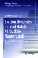
Figure 1.2 Halide perovskite family tree. Schematic illustration of standard 3D perovskite and the low-dimensional derivates, including Ruddlesden–Popper 2D, Dion–Jacobson 2D, “Pillar”-perovskite 1D, “Dot”-perovskite 0D, and the double perovskite pseudo-0D perovskite.
1.3 Property and Application of Perovskite Early research on perovskite oxides focused on the biaxial optical properties and ferroelectric properties. In contrast, halide perovskites open the door to studying the optoelectrical properties because of their unique electronic structures, including direct tunable bandgap, strong absorption, small and balanced electron-hole effective masses, and defect resistance, thereby improving their photoluminescence quantum yield. Moreover, the unprecedented flexibility of perovskite composition can be brought about by organic or inorganic components with optical or electronic functionalities. The most important advantage of halide perovskites is their facile, accessible, high-quality crystals and films, enabling structure–property correlation exploration and prototype device optimization. Thus, halide perovskite semiconductors will hold promise for a variety of fascinating applications, including photovoltaics (PVs), LEDs, photodetectors, memristors and lasers, see Figure 1.3, just to cite the ones that probably receive more attention. In addition to this versatility, it is important to highlight the enormous potential for the development of high-performance devices on flexible substrates, extending the application range of high-performance rigid photovoltaics.
1.3 Property and Application of Perovskite
Solar cell h
Metal anode HTL
V
Perovskite ETL Transparent cathode
Memristor
LED
e
e
e L rrie ong r li fet im ca
Defect resistance
L
Perovskite Substrate
an
ETL
od
al et M
an
Perovskite
S ab trong sor ptio n
r
e as
al et
HTL Transparent cathode
ble na p Tu dga n ba
cile Fa sible es acc
Laser
M
Flexibility composition
Perovskite Electrode Substrate
e
od
Metal electrode
Emission
Photodetector Irradiation c
le
e al et
de tro
M
de ro
ct
le
e al et
M
Perovskite
Flexible device
Substrate
Metal anode HTL
te
ki
rent Transpa thode ca flexible
vs ro Pe
ETL
Figure 1.3 Example of properties and applications of halide perovskite. Halide perovskites are promising semiconductors with excellent properties, including flexible composition, facile accessibility, tunable bandgap, strong absorption, long carrier lifetimes, and defects resistance. These merits enable halide perovskite to be competent in solar cells, LEDs, photodetectors, memristors, and lasers. Interestingly, halide perovskite devices can also be developed on flexible substrates due to the good performance of polycrystalline films and low-temperature growth conditions.
The organic–inorganic halide perovskites have received wide attention, mostly due to their high efficiency and low cost in next-generation PVs, which have made these materials start to compete with commercial thin-film cells. Such materials harvest the energy of sunlight efferently because of their high absorption coefficients in both visible and near-infrared light. The first report of the perovskite solar cell was in 2009 [16], and now the record laboratory-scale power conversion efficiency of perovskite film is certified at 25.7% (https://www.nrel.gov/pv/cell-efficiency). Perovskite film-based solar cells are easy to be fabricated at low temperature, more energy-saving, and environmentally friendly than the conventional silicon wafer with a lower payback time [17], but with a lower contrasted long- term stability.
5
6
1 Introduction to Perovskite
Consequently, further commercialization process of perovskite-based solar cells has been hindered by the stability problem, including degradation due to moisture, oxygen, heat, light, mechanical stress, and reverse bias. These failings do not detract from the overall excellence but focus the research effort on increasing device stability. Halide perovskite materials remain a cost-effective solution to address vast electrical energy supplies. While initial boost of halide perovskite research was the development of photovoltaic devices, the good performance of these solar cells is founded on low nonradiative recombination, which is also beneficial for other optoelectronic devices. Consequently, halide perovskites are also currently impacting the development of a broad range of optoelectronic devices and systems. One significant benefit of halide perovskites used as LEDs is their very high color purity, with full width at a half-maximum of 20 nm for the blue or green–blue electroluminescence spectrum peaks [18]. Unlike traditional inorganic nanomaterials, the exceptional color purity of quantum-well nanoparticles is maintained regardless of crystal size. As a result, halide perovskites have the potential to solve some of the drawbacks of existing LEDs, such as difficult synthesis challenges, high cost, poor color purity of organic LEDs, and high ionization energy of quantum dot LEDs. Since the first demonstration of perovskite LEDs in 2014, the external quantum efficiency (EQE) of these devices has rapidly increased from below 1% to 25.8% for red [19], 28.1% for green [20], and 14.8% for blue [21]. The new LED technology has seen a meteoric rise in device efficiencies, but many scientific and technical obstacles, such as the unsatisfied stability and efficiency of blue LEDs, still stand in the way of perovskite LEDs further advancement into real-world applications. Halide perovskite-based photodetectors exhibit comparable performance to commercially available photodetectors based on crystalline Si and III–V, offering significant potential for the technology of light-signal detection. The outstanding intrinsic optoelectronic properties of halide perovskites, such as photoinduced polarization, high drift mobilities, and effective charge collection, have contributed to the current growth of cutting-edge material studies in the field of light-signal detection. Halide perovskite semiconductors feature effective light absorption, enabling the detection of a wide range of electromagnetic waves from ultraviolet and visible to near-infrared and even radiations (X-ray, γ-ray, etc.), with low-cost solution processability and high photon yield. This class of semiconductors may empower ground-breaking photodetector technology in the areas of imaging, optical communications, and biomedical sensing; in this last case, further stability in polar solvent media, such as water, could increase enormously the range of applications of these systems. Moreover, halide perovskites present a high ionic bonding character and ionic conductivity, causing the coexistence and coupling of ionic and electronic components of current and capacitance. This fact is at the base of nonconventional effects on optoelectronic systems, which could be a source of instabilities but can also be exploited. In this sense, halide perovskites exhibited good memristive properties supported by their electronic–ionic conductivity properties [22]. Memristor, that is memory resistor, is a leading candidate with robust capabilities in information storage and neuromorphic computing applications to address the growing challenge of approaching the end of Moore’s law and the von Neumann bottleneck. The memristive property of halide perovskite is achieved through the synergistic coupling of
References
photonic, electronic, and ionic processes, which enable perovskite to demonstrate novel functions such as optical-erasing memory, optogenetically inspired synaptic functions, and light-accelerated learning with multifunctionalization and novel photonic, logical, multilevel, and flexible functions. Aside from the above-mentioned, halide perovskites have much more extensive applications due to their outstanding attributes, such as lasers, X-ray detectors, waveguides, scintillators, gas sensors, spintronics, and photocatalysis.
1.4 Summary and Outlook The last two decades have seen the rapid development of halide perovskite materials, with researchers in particular pioneering systematic structural and property correlation studies based on halide perovskite composition and phases. The structure of perovskites has also been derived from ABX3 to various derivatives that are important for changing chemical properties, controlling energy bands, and granting new physical properties. Perovskite materials, as an excellent new generation of semiconductor materials, have been demonstrated to be useful in a wide range of application scenarios, including photovoltaics, displays, and sensing, storage. However, the environmental and thermodynamic stability of halide perovskitebased applications are two major challenges impeding their development, and some related phenomena and mechanisms should be thoroughly investigated to address perovskite device long-term use problems. Scientists have begun to use multimodal characterization to study the structural changes of halide perovskites, to monitor structural changes related to physical processes using in situ technology, and to conduct large-scale studies to establish correlations between components and properties using AI technology. The halide perovskite is like a treasure trove, and more interdisciplinary collaboration will lead to even more unexpected discoveries. This book will overview the intriguing properties of halide perovskites, making this system significantly different from other optoelectronic materials. Properties of materials and devices will be overviewed as well as the perspective on material and device development, always focusing on the fundamental properties.
References 1 Wainer, E. (1946). High titania dielectrics. Transactions of the Electrochemical Society 89 (1): 331. 2 Miyake, S. and Ueda, R. (1932). On polymorphic change of BaTiO3 . Journal of the Physical Society of Japan 1 (1): 32. 3 Cross, L. and Newnham, R. (1987). History of ferroelectrics. Ceramics and Civilization 3: 289. 4 Wells, H.L. (1893). Über die cäsium-und kalium-bleihalogenide. Zeitschrift für anorganische Chemie 3 (1): 195. 5 Møller, C. (1957). A phase transition in cæsium plumbochloride. Nature 180 (4593): 981.
7
8
1 Introduction to Perovskite
6 Møller, C. (1958). Crystal structure and photoconductivity of caesium plumbohalides. Nature 182 (4647): 1436. 7 Weber, D. (1978). CH3 NH3 PbX3 , ein Pb(II)-system mit kubischer perowskitstruktur/CH3 NH3 PbX3 , a Pb(II)-system with cubic perovskite structure. Zeitschrift für Naturforschung B 33 (12): 1443. 8 Weber, D. (1978). CH3 NH3 SnBrx I3−x (x = 0–3), ein Sn(II)-system mit kubischer perowskitstruktur/CH3 NH3 SnBrx I3-x (x = 0–3), a Sn(II)-system with cubic perovskite structure. Zeitschrift für Naturforschung B 33 (8): 862. 9 Mitzi, D., Wang, S., Feild, C. et al. (1995). Conducting layered organic-inorganic halides containing⟨110⟩-oriented perovskite sheets. Science 267 (5203): 1473. 10 Mitzi, D.B. (1999). Synthesis, structure, and properties of organic-inorganic perovskites and related materials. In: Progress in Inorganic Chemistry (ed. K.D. Karlin). 11 Mitzi, D.B. (2000). Organic-inorganic perovskites containing trivalent metal halide layers: the templating influence of the organic cation layer. Inorganic Chemistry 39 (26): 6107. 12 Goldschmidt, V.M. (1926). Die Gesetze der Krystallochemie. Naturwissenschaften 14 (21): 477. 13 Han, G., Hadi, H.D., Bruno, A. et al. (2018). Additive selection strategy for high performance perovskite photovoltaics. The Journal of Physical Chemistry C 122 (25): 13884. 14 Li, C., Lu, X., Ding, W. et al. (2008). Formability of ABX3 (X = F, Cl, Br, I) halide perovskites. Acta Crystallographica Section B 64 (6): 702. 15 Mao, L., Ke, W., Pedesseau, L. et al. (2018). Hybrid Dion–Jacobson 2D lead iodide perovskites. Journal of the American Chemical Society 140 (10): 3775. 16 Kojima, A., Teshima, K., Shirai, Y., and Miyasaka, T. (2009). Organometal halide perovskites as visible-light sensitizers for photovoltaic cells. Journal of the American Chemical Society 131 (17): 6050. 17 Vidal, R., Alberola-Borràs, J.-A., Sánchez-Pantoja, N., and Mora-Seró, I. (2021). Comparison of perovskite solar cells with other photovoltaics technologies from the point of view of life cycle assessment. Advanced Energy and Sustainability Research 2 (5): 2000088. 18 Adjokatse, S., Fang, H.-H., and Loi, M.A. (2017). Broadly tunable metal halide perovskites for solid-state light-emission applications. Materials Today 20 (8): 413. 19 Jiang, J., Chu, Z., Yin, Z. et al. (2022). Red perovskite light-emitting diodes with efficiency exceeding 25% realized by co-spacer cations. Advanced Materials 34 (36): 2204460. 20 Liu, Z., Qiu, W., Peng, X. et al. (2021). Perovskite light-emitting diodes with EQE exceeding 28% through a synergetic dual-additive strategy for defect passivation and nanostructure regulation. Advanced Materials 33 (43): 2103268. 21 Shen, Y., Li, Y.-Q., Zhang, K. et al. (2022). Multifunctional crystal regulation enables efficient and stable sky-blue perovskite light-emitting diodes. Advanced Functional Materials 32 (41): 2206574. 22 John, R.A., Shah, N., Vishwanath, S.K. et al. (2021). Halide perovskite memristors as flexible and reconfigurable physical unclonable functions. Nature Communications 12 (1): 3681.
9
2 Halide Perovskite Single Crystals Clara Aranda-Alonso 1,2 and Michael Saliba 1,2 1 2
Institute for Photovoltaics (IPV), University of Stuttgart, 70569 Stuttgart, Germany IEK5-Photovoltaics, Forschungszentrum Jülich, 52425 Jülich, Germany
2.1 Introduction To further explore the potential of hybrid halide perovskite materials, including solar cells and beyond, their optoelectronic properties still need to be thoroughly investigated. In this respect, single crystals (SC), with fewer defects, are the ideal candidates to further analyze these properties without the detriment of the instability under atmospheric conditions that polycrystalline perovskites exhibit. In this chapter, we address the main characteristics and applications of SC based on perovskite materials. The chapter is organized as follows: first, the three principal perovskite crystal structures are described, distinguishing between lead-based, lead-free, and all inorganic perovskite single crystals. Then, the different synthesis methods are described, highlighting the ones with significant impact. To further understand the potential of this material, the optoelectronic properties of the most commonly used SC are discussed in depth. Finally, the main applications of these materials in different technologies are described, including their abilities as photodetectors, scintillators, solar cells, light emitting diodes, and memristors.
2.2 Crystal Structure In the general perovskite oxide structure, ABX3 , A and B are cations of different sizes. A used to be larger than B, being B six-coordinated by an X-site anion to form a BX6 octahedron complex. To arrange a three-dimensional (3D) system, the octahedron must share the corners, locating A-cations in the cavities of the framework. The charge of each cation and anion must be such as to preserve electroneutrality. In the hybrid perovskite materials, the A-cation is a monovalent organic amine, B is a divalent metal (Pb2+ , Sn2+ ) and X is the halide element (I− , Br− , and Cl− ), or an extended version associating molecular linkers (azides N3− , cyanides CN− , or even borohydrides BH4− ). The divalent metal could also be replaced by mixed monovalent and trivalent metals, forming double perovskites A2 BB′ X6 structures. As well as Halide Perovskite Semiconductors: Structures, Characterization, Properties, and Phenomena, First Edition. Edited by Yuanyuan Zhou and Iván Mora-Seró. © 2024 WILEY-VCH GmbH. Published 2024 by WILEY-VCH GmbH.
10
2 Halide Perovskite Single Crystals
for their polycrystalline counterparts, the capability of tuning the chemistry of perovskite single crystals is governed by the ionic ratio sizes of their components. The Goldschmidt tolerance factor (t) and the octahedral factor (𝜇) should be considered to design a stable and useful perovskite material. In Sections 2.2.1, 2.2.2, and 2.2.3, we will summarize the structure of the most commonly used perovskite formulations for SC growth, including lead-based, lead-free, and all inorganics.
2.2.1
Lead-Based Perovskite Single Crystals
In Pb-based halide perovskites, crystallization occurs in the ABX3 structure, which is isostructural to the initial perovskite oxide CaTiO3 . The A and B cations coordinate with 12 and 6 X anions, leading to the 3D corner-sharing cuboctahedral (12-fold coordinated) and octahedral (sixfold coordinated) structures. In the MAPbX3 structure, the methylammonium position is disordered in the tetragonal phase from 160 K to room temperature, whereas it is ordered below 160 K in the orthorhombic phase (Figure 2.1) [1]. Lead-based perovskite single crystals are the most studied to date. They correspond to the perovskite structures that have given record efficiency results in thin film solar cells. Thus, the information that can be extracted from the bulk of these materials will also be valuable for research on thin films. On the other hand, they can be synthesized by a wide range of methods, some of which are fully described in Section 2.3. Examples of different lead-base perovskite single crystals already grown are shown in Figure 2.2 [2]. It is well known that temperature influences the structural transitions of perovskite materials, having a direct impact on their optoelectronic properties. It is then essential to clarify the relationship between both phenomena in perovskite single crystals to understand their polycrystalline counterparts further as well. Ding and coworkers reported a depth analysis of the different crystal facets of MAPbI3 single crystal. They confirm the different atom densities for the different facets and how this influences ionic migration [3]. In Figure 2.3a, the X-ray diffraction (XRD) pattern of facet (100) of both single crystal and powder diffraction is shown. Cubic
Tetragonal
Orthorhombic
b
b
MAPbI3 MAPbBr3 0.85 MAPbCl3 MASnI3
b
MASnBr3 MASnCl3
c
c
FAPbl3 0.90
c
FAPbBr3 FAPbCl3
FASnl3 FASnBr3
a
a
a=b=c CH3NH3+ (MA cation)
(a)
a=b≠c +
Pb (Lead cation)
a
FASnCl3
a≠b≠c
0.95
I– (Lead cation)
Tolerance factor (t)
(b)
Figure 2.1 (a) Crystal structures for MAPbX3 single crystals. Cubic, tetragonal, and orthorhombic groups. (b) Tolerance factors for the different perovskite compositions, Pb and Sn containing. Source: Reproduced with permission from Murali et al. [1]/American Chemical Society.
2.2 Crystal Structure
MAPbCl3
FAPbl3
MAPbl3
MAPbBr3
10
20
40
(310)
(220)
40
(300)
(211)
30 2θ (°)
30
(b)
001
(200) (210) (110) (111)
60
2θ (°)
20
(200)
(440)
50
(600)
10
(404)
(114) (220) (310) (312) (321) (400) (314) 40
30
Powder
(100)
(100) Intensity (a.u.)
(600)
20
10
(a)
Intensity (a.u.)
(100) plane
(200) (202) (004)
(200) (211)
(002) (110)
Intensity (a.u.)
(400)
Figure 2.2 Photographs of Pb-based perovskite SCs: MAPbCl3 , MAPbBr3 , MAPbI3 , and FAPbI3 Source: Reproduced with permission from Liu et al. [2]/John Wiley & Sons.
50
50
2θ (°)
MAPbCl3
002 011
021 211 111
10
(c)
20
30 2θ (°)
40
003 123 022 031 222 113 50
Intensity (a.u.)
Intensity (a.u.)
FAPbl3
MA0.45FA0.55Pbl3
MAPbl3
10
60
(d)
15
20
25
30
35
40
2θ (°)
Figure 2.3 X-Ray diffraction patterns from the most commonly used lead-based perovskite structures. (a) MAPbI3 . Source: Reproduced with permission Ding et al. [3]/American Chemical Society. (b) MAPbBr3 single crystal. Source: Reproduced from Wang et al. [4]/Springer Nature/CC BY 4.0. (c) MAPbCl3 single crystal. Source: Reproduced from Lee et al. [5]/MDPI/CC BY 4.0. (d) Mixed MA and FA lead iodide single crystal stabilized. Source: Reproduced with permission from Li et al. [6]/Royal Society of Chemistry.
In the case of MAPbBr3 , the crystal belongs to the cubic Pm3m space group at room temperature, as seen in Figure 2.3b from both single crystal and powder diffraction methods. However, the crystal experiences several structural transitions with lowering temperatures, from cubic to tetragonal, tetragonal to orthorhombic I, and orthorhombic I to orthorhombic II [4]. But this composition is not the only one suffering from this temperature instability; MAPbCl3 (Figure 2.3c) also shows two structural phase transitions: (i) from the cubic-to-tetragonal phase at around −95 ∘ C and (ii) from the tetragonal to the orthorhombic when lowering to −116 ∘ C [5].
11
12
2 Halide Perovskite Single Crystals
The room-temperature instability of the FA derivatives is well-known in polycrystalline devices, and their monocrystalline partners are not spared either. FAPbI3 perovskite transforms from cubic phase to non-perovskite phase, making its practical application difficult. Kuang and coworkers stabilized the black phase (cubic) by adding MA to the precursor solution. The XRD pattern of the mixed MA0.45 FA0.55 PbI3 perovskite single crystal, stable for 14 days, is shown in Figure 2.3d [6].
2.2.2
Lead-Free Perovskite Single Crystals
Pb-free SCs presume a variety of crystal structures, which are not necessarily limited to the typical ABX3 architecture. The replacement of Pb2+ ions leads to a nanoscale deformation and a depth change in the optoelectronic properties due to the differences in chemical valence and ionic size. In this case, the crystal structure depends mainly on substitutions, including group-14 elements (Sn and Ge), adjacent elements such as Sb or Bi, and double elements (i.e. Bi combined with Ag) [7]. These substitutions extend from orthorhombic to trigonal lattice systems, generating quaternary structure A2 B+ B3+ X6 . A vacancy-ordered double perovskite can also be synthesized by removing part of the B atoms from the octahedron center. Isolated clusters can be obtained using transition or post-transition elements to form two face-sharing [M2 X9 ]3− octahedra. Below is a summary of the possible substitutes for lead to develop lead-free perovskite single crystals (Figure 2.4).
Figure 2.4 Diagram of the main routes to replace Pb in perovskite crystals. Source: Reproduced with permission from Zhang et al. [7]/John Wiley & Sons.
2.2 Crystal Structure
2.2.3 All-Inorganic Perovskite Single Crystals If perovskite does not contain any organic component, it can be categorized as all-inorganic perovskite. The main advantage of this inorganic variant is the absence of organic cations due to their associated intrinsic instability. Therefore, the all-inorganic perovskites show impressive thermal and environmental stability, opening new ways to further applications with limited restrictions. Regarding the structure, all-inorganic perovskite single crystals can be divided into three main categories: ABX3 type, special structures, and doped perovskites (Figure 2.5) [8]. Regarding the traditional ABX3 type, the principal protagonist lacking lead is the CsPbBr3 formulation. This inorganic single crystal is grown by the Bridgman method (described in Section 2.3) and the solution-grown method. He et al. optimized the growth conditions using the Bridgman method, considering the relation between the crystal’s defects and an excessive temperature gradient [9]. After thoughtful optimization, CsPbBr3 with high purity was obtained,
A2BB′X6 Type Double PSC
Lowdimensional Type PSC 5 mm
All-inorganic PSCs 4 mm
X/γ-rays
[NaCl6]5–
ABX3 Type PSC
[FeCl6]3– [AgCl6]5–
Mixed Type PSC
Cs+
Figure 2.5 Summary of all-inorganic PSC: ABI B III X6 type, low-dimensional type, mixed type, and ABX3 traditional type PSC. Source: Reproduced from Wu et al. [8]/MDPI/CC BY 4.0.
13
14
2 Halide Perovskite Single Crystals
performing as a great gamma-ray detector. Their work reported that CsPbBr3 exhibits two nondestructive phase transitions at low temperatures. The transition first occurs around 130 ∘ C, from a cubic to tetragonal system. This is followed by a second-order transition at around 88 ∘ C to the orthorhombic phase, which is stable at room temperature. Another structure that shows high stability in air and excellent optoelectronic properties is TlPbI3 . This material has a low melting temperature, which reduces the thermally activated defects during growth of the process, which is typically the Bridgman method. Several improvements have been made to exploit this material’s full potential as a gamma-ray detector [10]. CsSnI3 SCs have shown p-type metallic behavior, presenting the highest hole mobility among the p-type semiconductors. Chung et al. applied doped CsSnI3 to solar cells, developing all-solid-state dye-sensitized solar cells with outstanding PCE of up to 10.2% [11].
2.3 Synthesis Methods The synthesis of crystals can be classified into three groups: solid–solid, liquid–solid, and gas–solid methods, depending on the phase transition that occurs during the growing process. Most technological crystals are obtained through the liquid–solid mechanism, including perovskite single crystals. In this section, the most widely used synthesis methods included in this category are summarized.
2.3.1 Antisolvent Vapor-Assisted Crystallization (AVC) Method Antisolvent vapor-assisted crystallization (AVC) method provides high-quality perovskite single crystals at room temperature, reducing energy consumption. It is a process that has been used for preparation of micro- and nanoparticles for several years. This method’s key parameter is the solubility of the perovskite precursor solution in different solvents. A solvent–solute system is formed, where on one hand there is the couple formed by the solute and the solvent (precursor solution), and then is the antisolvent (AS), which is perfectly miscible with the solvent but in which the solute is insoluble. When the AS diffuses across the perovskite precursor solution, the solubility of the solute drastically decreases, leading to the crystallization of the material as a precipitate (Figure 2.6). To properly visualize the method, let us take the MAPbBr3 crystal as an example. The first step is to dissolve the perovskite precursors, MABr and PbBr2 , in a molar ratio of 1 : 1 in a commonly used solvent, dimethylformamide (DMF). This will be the precursor solution. This solution will then be placed in a small vial sealed under the atmosphere of the antisolvent, i.e. dichloromethane (DCM), which will diffuse into the perovskite solution, forming the crystals. Depending on the nature of the perovskite precursors, the solvents and the AS can vary between DMF, gamma-butyrolactone (GBL), or dimethyl sulfoxide (DMSO). The options for choosing AS are quite wide if the insolubility of the solute is ensured. As might
2.3 Synthesis Methods
AS diffusion
Single crystals
PVK solution
Figure 2.6 Schematic illustration of the antisolvent vapor-assisted crystallization (AVC) method. Source: Clara Aranda-Alonso.
be expected, the speed of the crystal growth is proportional to the diffusion rate of the AS into the solution. However, the reproducibility of this method can be challenging, constituting a constraint for large-scale processing.
2.3.2
Solution Temperature Lowering (STL) Method
In the case of solution temperature lowering (STL), the change in the solubility of perovskite precursors in acid halide solvents (e.g. HI, HBr, and HCl) due to different temperatures is the protagonist. The first step is to dissolve the perovskite precursors at high temperature, and then the solution is progressively cooled down. This process leads to a supersaturated solution, which promotes the crystal’s growth. The STL method has two variants as a seed-assisted method: (i) crystal seed at the bottom (BSSG) of a vial containing the stock solution, or (ii) on the top (TSSG), suitably fixed as illustrated in Figure 2.7. In the case of BSSG-type growth, immersing the seed in the solution shall be repeated as many times as necessary until the desired crystal size is achieved. For TSSG, small seeds need to be fixed on a substrate and immersed in the top half of the
Large single crystal
Tª
Tª
Tª Seed crystal
Seed crystal
Figure 2.7 Schematic representation of the solution temperature lowering (STL) method. Source: Clara Aranda-Alonso.
15
16
2 Halide Perovskite Single Crystals
Thermotank Cooling CH3NH3I + Pb(AC)2.3H2O in HI solution CH3NH3PbI3 seed crystal
(a)
(b)
(c)
Silicon substrate Air cooling CH3NH3PbI3 seed crystal
CH3NH3+Pb2+I– Small crystal Hot plate
(d)
(e)
Figure 2.8 Schematic diagram of STL crystallization. (a–c) Crystallization process of BSSG and images of as-prepared CH3 NH3 PbI3 single crystal; (d, e) TSSG method and the obtained crystal [12]. Source: (b) Dang et al. (2015)/Royal Society of Chemistry. (c) Lian et al. (2015)/ Springer Nature/CC BY 4.0.
precursor. The lower half of the solution containing the seed is heated in an oil bath. The upper half is cooled with air to create a temperature gradient, inducing crystallization. At the same time, a convection current providing ions is produced in the lower half. With this method, large single crystals can be obtained by strictly controlling the temperature. An example of this growing method is shown in Figure 2.8 [12]. However, it is not suitable for crystals with low solubility at elevated temperatures. The prolonged rate of growth is also a disadvantage, together with the formation of by-products such as MA4 PbX6 ⋅2H2 O and irregular crystals if the temperature drops too fast.
2.3.3 Bridgman Method With the Bridgman technique, large single perovskite crystals can be grown. This solid–solid technique’s operation mechanism is based on the crystal’s growth inside a sealed quartz ampoule. This ampoule is placed inside a furnace filled with an inert atmosphere or vacuum, allowing a temperature gradient. The polycrystalline material (powdered or seed) is first heated above its melting point, and then the temperature is gradually reduced from the one end where the seed is located. Then, the crystallization front propagates through the molten material. The final crystal will have the same geometry as the vessel containing it (Figure 2.9a). This method has been historically used for semiconductor crystals, such as GaAs, ZnSe, CdS, and CdTe. This method is valid if the melting points of the compounds to be crystallized are defined. In fact, it is not possible to use organic compounds, which are chemically unstable at their melting point.
2.3 Synthesis Methods
Gas out
Direction of motion
Molten materials
Bridgman crystals
(a)
Gas in
(b)
Figure 2.9 (a) Schematic explanation of the Bridgman crystallization method. (b) CsPbBr3 perovskite single crystal grown by the BM. Source: Reproduced with permission from Zhang et al. [13]/John Wiley & Sons.
Another limitation of this method is that the crystal grows along the walls of the ampoule, which can lead to several defects due to the mechanical stress. The defects that may appear include small grain boundaries in the crystals, reducing their purity and their potential for technological applications. In addition, the crystallization parameters, such as the temperature gradient, dropping speed, and cooling rate, need to be well controlled to avoid cracks in the ingots. One of the examples of single perovskite crystals grown through this method was reported by Zhang et al. [13]. They developed a simplified version of the method using a homemade vertical two-zone furnace. The large crystal of CsPbBr3 is shown in Figure 2.9b.
2.3.4 Slow Evaporation Method The slow evaporation method is a liquid–liquid technique, which uses a controlled rate of solvent evaporation from a solution precursor close to the saturated state. As we said before, this saturated state represents the driving force and can be achieved by a change in temperature or by the solvent evaporating (Figure 2.10A). The steady-state nucleation rate on the crystal surface is defined as: ( ) ΔG∗ j0 = 𝜔∗ ΓN0 exp − kB T
17
2 Halide Perovskite Single Crystals
Slow evaporation – soultion growth method
Evaporation holes
Mixed solution Time in days
(A)
Crystals
Beakers
(a)
(b)
Controlled evaporation
5 mm
PEABr+PbBr2 in DMF (d)
8.0 .7
7
Crystallization
m
g
h–1
7.5
1.0 –2 .89
mg
7.0 h–1
0.9 0
(B)
6.5
Unsaturated zone
100
200
300
Time (h)
400
500
101 Mass of solution (g) Mass of SCs (g)
–3
101
2.7 + 0.28 mg h–1
100
100
10–1
10–1
10–2
10–2
10–3
10–3
200
250
300
350 400 Time (h)
450
Growth rate (mg h–1)
(c) 1.1
Concentration (g ml−1)
18
500
Figure 2.10 Top: (A) Schematic representation of the slow evaporation method. Bottom: (B) Example of the method applied to the growth process of (PEA)2 PbBr4 single crystals. (b) Photograph of a transparent, ∼27 × 11 mm2 (PEA)2 PbBr4 single crystal. (c) Mass and concentration of (PEA)2 PbBr4 precursor solution as a function of evaporation time. (d) Mass and growth rate of (PEA)2 PbBr4 as a function of time. Source: Reproduced with permission from Zhang et al. [14]/Royal Society of Chemistry.
where 𝜔* is the frequency at which the solute molecules diffuse from the solution to the critical nucleus, Γ is the nonequilibrium Zeldovich factor, N 0 is the density of adsorption sites, ΔG* is the Gibbs free energy change for the nucleus formation, kB is the Boltzmann constant, and T is the temperature. This equation defines the existence of a supersaturation level below which the nucleation rate becomes zero and increases rapidly above it. Attending to the exponential term, to achieve only the required high-quality single crystal, the growth conditions need to be controlled by regulating the temperature. This crystallization technique represents one of the simplest methods to grow organic crystals, both in 3D and 2D architectures. Zhang and coworkers reported an
2.3 Synthesis Methods
example of 2D perovskite single crystal grown by this method in 2019 (Figure 2.10B) [14]. They developed an optimized growing process leading to a well-defined large-size (>200 mm2 ) 2D (PEA)2 PbBr4 (C6 H5 CH2 CH2 NH3 + , PEA+ ) single crystals. The excellent performance of the synthesized crystals made them very ideal for ultrafast optical computing and optical communications, reaching the quality of the state-of-the-art materials such as ZnO, TiO2 , and GaN in the field.
2.3.5 Inverse Temperature Crystallization (ITC) Method As the name suggests, this method is based on the phenomenon that solubility is inversely proportional to temperature. Also known as retrograde solubility, this process describes the change in a solute concentration above the eutectic temperature (Figure 2.11a) [15]. The effects that this phenomenon can cause are clear: high enthalpy, variable distribution coefficient, and maximum chemical potential. However, A. L. McKelvey in 1996 described the origin of this mechanism from a thermodynamic point of view. That work concluded that retrograde solubility could occur if the ΔH mix is large enough to cause a miscibility gap in ΔGmix at temperatures larger than the eutectic temperature (the subindex mix refers to the MAPbBr3 solubility in DMF
Solubility (g m−1)
0.7
Eutectic T
T
0.6 0.5
20%
34%
60
80
48%
1M solution
0.4 0.3
20
XA, max B
A (a)
40
100
Temperature (°C)
(b)
Heating to a fixed temperature Solution
Oil bath
Room temperature
Fast crystallization
Solution + MAPbX3 crystals
Oil bath
Hot plate
(c)
Figure 2.11 (a) Schematic phase diagram showing the phenomenon of retrograde solubility and the solubility maximum above the eutectic temperature. Source: Reproduced with permission from Mckelvey [15]/Springer Nature. (b) Temperature-dependent solubility of MAPbBr3 in DMF shows yield at different temperatures. Source: Reproduced with permission from Saidaminov et al. [16]/Royal Society of Chemistry. (c) ITC setup in which the crystallization vial is heated from room temperature and kept at an elevated temperature. Source: Reproduced with permission from Saidaminov et al. [17]/Springer Nature/CC BY 4.0.
19
20
2 Halide Perovskite Single Crystals
mixture of components in the solution; ΔH mix and ΔGmix are the enthalpies and the free energy of the mixing). It was established that this effect can occur in any binary system where the enthalpy dominates the free energy of mixing above the given temperature invariant. Few cases of materials presenting this effect have been reported so far; luckily, perovskite is one of them. Bakr and coworkers demonstrated this when they observed an apparent solubility decrease of MAPbX3 perovskites in the habitual solvents (DMF, GBL, etc.) with increasing temperature [17]. The inverse solubility does not occur with all solvents. For instance, in the case of MAPbBr3 , this phenomenon is clear for DMF (Figure 2.11b), but does not happen using DMSO [16]. The reason behind this is the different coordination capabilities of both within the lead halide precursor. In the case of DMSO, this capability is much higher, leading to a stronger binding with the lead. Once the solvent is chosen considering this premise, the second thing to do is control the temperature and concentration of the solution. The result will depend strongly on that. The setup to execute the method is easy: just a vial containing the precursor solution and a hotplate coupled with a precise temperature controller (Figure 2.11c) [17]. This method allows the growth of high-quality perovskite single crystals and drastically reduces the synthesis times. If the temperature is higher than the needed one, the process’s speed will increase, leading to multiple small crystals. Then, it is crucial to maintain a balance between the ramp temperature and concentration. Once the crystal is grown, it is important to isolate it outside the solution; if the temperature decreases to room temperature while the crystal is inside, it will redissolve. A variant of this method involves using a seed to obtain larger crystals with further control of shape and size. This works by carefully taking the crystal and placing it in a fresh precursor solution. A comparison between seeded and unseeded MAPbBr3 single crystals using this ITC method is shown in Figure 2.12. This method is suitable for different perovskite formulations such as FAPbI3 , MAPbCl3 , MAPbIx Br1–x , and MAx FA1–x PbI3 crystals.
2.3.6
Methods for 2D and 1D Perovskite Single Crystals
Quasi-2D perovskites known as Ruddlesden–Popper (RP) perovskites, have the structural formula as A2 Bn−1 Mn X3n+1 , where A is a long-chain alkyl or aromatic group, B is a small organic cation, M is a divalent metal, and X is a halogen. The index n is the number of the 3D system layers inserted between the two layers of A+ cations. This process is tunable by controlling the precursor’s stoichiometry during the synthesis. In this low-dimensional system, the layers of A+ cations have the role of “barriers” for carriers due to the large bandgap. On the other hand, in the 3D system, there are the B+ cations, which serve as “wells.” The wells’ thickness in these quantum well structures is determined by the index n, which can be easily tailored. ITC and AVC methods widely used for 3D structures are not feasible to grow 2D perovskite SC. Instead, cooling temperature appears to be an effective method to reduce the solubility of a saturated solution.
2.4 Optoelectronic Properties of Halide Perovskite Single Crystals
(a)
(d) (b)
(c)
Figure 2.12 (a–c) Real pictures of MAPbI3 , MAPbBr3 , and MAPbCl3 single crystals grown through unseeded ITC method. (d) MAPbBr3 single crystal grown by the seeded assisted ITC method. Notice the boundaries of the seeded one demonstrating the dimensions control. Courtesy of Waqas Zia.
An example can be found in the work reported by Kanatzidis and coworkers. With this method, they successfully obtained a 2D (BA)2 (MA)n−1 PbnI3n+1 (n = 1–4) SCs [18].
2.4 Optoelectronic Properties of Halide Perovskite Single Crystals Perovskite single crystals have demonstrated their potential to be applied in various technologies such as photodetectors, X-ray or γ-ray detectors, high-performance solar cells, or light emitting devices. This is possible due to the optoelectronic properties of these materials in their monocrystalline phase, which are mainly characterized by the absence of grain boundaries. These properties: large carrier diffusion length, long carrier lifetime, extended absorption range, and low carrier defects. In this section, we will summarize these properties, highlighting the instrumental techniques used to understand them.
2.4.1 UV–Vis Absorption, Photoluminescence (PL), and Transient Decays: TRPL and TPV As mentioned above, the main characteristic of single crystals is that they lack of grain boundaries. It is precisely this feature that gives them optoelectronic properties
21
2 Halide Perovskite Single Crystals
that are in several aspects different from those of their polycrystalline counterparts. One of the main consequences of this is a decrease in charge recombination. On the other hand, the highly ordered pattern in perovskite single crystal lattice significantly reduces the charge carrier trapping, favoring a long carrier diffusion length which is defined as follows: √ kT 𝜇𝜏 LD = q where k is the Boltzmann constant, T the absolute temperature, q the elementary charge, 𝜇 the carrier mobility, and 𝜏 the carrier lifetime. This property will define the architecture and composition of the device containing the single crystal. The absorption range of single perovskite crystals is redshifted compared with the polycrystalline films (Figure 2.13) [19]. This is caused by enhanced below-bandgap absorption and a clear band edge cutoff with no excitonic signature. This is also a signal of low defect states. In the case of MAPbI3 single crystals; below-bandgap absorption is detected, originating in a weakly indirect bandgap of ≈60 meV below
MAI
MACl MAPbBr3
MAPbCI3
MAPbl3 MABr
MABr
MAPbBr3–xlx
MAPbBr3–xClx
x 2
3
1.5
1
0.5
0
0.5
1.5
1
x 2
3
MAPbBr3–xClx
2.5
x=3
3.0
x=0
x=3
x=3
x=0
x=3
[F(R)hv]2
MAPbBr3–xlx Absorption (a.u.)
22
2.0 hv (eV)
Figure 2.13 Tunable bandgaps in perovskite single crystals. The absorption spectra redshifted is also shown. Source: Reproduced with permission from Jang et al. [19]/American Chemical Society.
1.5
2.4 Optoelectronic Properties of Halide Perovskite Single Crystals
the direct bandgap transition. The absorption coefficient of the below-bandgap transition is several orders of magnitude smaller than that of the above-bandgap transition, resulting in negligible below-bandgap absorption in polycrystalline perovskite films but obvious in SCs due to the thicker thickness and larger carrier diffusion length. The extended absorption range makes more photons absorbed and increases the short-circuit current density when applied to solar cells, for instance. Regarding photoluminescence (PL), it has been demonstrated that single perovskite crystals show weaker PL in vacuum than in ambient conditions. This was attributed to the oxygen and water passivation of the crystal’s surface. Temperature-dependent XRD and PL have also been performed to analyze the phase transitions and trap states. In the case of MAPbBr3 , it was reported that a phase transition occurs from the orthogonal phase (Pna21) at 230 K. PL measurement and time-resolved photoluminescence (TRPL) measurement performed in single perovskite crystals, show that free excitons (FEs) have a short lifetime of nanoseconds and bound excitons (BEs) have a long lifetime of a few microseconds (Figure 2.13). Therefore, the TRPL spectra are visualized to verify that the highest energy level peaks originate from FEs, and the low energy level peaks originate from Bes, which are attributed to trap states [20].
2.4.2 Electronic Properties Like their polycrystalline counterparts, single perovskite crystals also stand out for their notable electrical properties. In this section, the electronic properties of perovskite monocrystalline devices are summarized through two main techniques: space charge limited current (SCLC) and impedance spectroscopy (IS). 2.4.2.1 Space-Charge-Limited Current (SCLC)
The SCLC is a steady-state technique to analyze the charge transport properties of a semiconductor [21]. The carrier mobility and trap density of single perovskite crystals are the two main properties that can be determined with this technique. The procedure is to record the dark current as a function of the applied voltage [22]. However, the data obtained from the SCLC model can easily be misinterpreted if the correct model is not selected considering the nature of the device [23, 24]. The most widely used SCLC method is based on the Mott–Gurney (MG) law (Eq. (2.1)) [25]. 9 V2 𝜀𝜇 8 L3 where 𝜇, 𝜀, and L are the charge carrier mobility, permittivity, and thickness of the perovskite semiconductor. To apply this model accurately, the device must satisfy some conditions: (i) The semiconductor material under study has to be undoped and trap-free, (ii) the configuration should be the sandwiched one, where the semiconductor is placed between two ohmic contacts, and (iii) the diffusion contributions to the current need to be insignificant, which can occur only for specific voltage ranges, also in the case of devices satisfying the two first conditions. If our system meets at J=
23
2 Halide Perovskite Single Crystals
JαV 2
Current density
24
JαV n>2
VTFL
JαV
Trap filling
Ohmic
Figure 2.14 The jV characteristics visualize different transport regions. A linear ohmic regime (JαV , blue line) is followed by the trap-filling regime, marked by a steep increase in current (JαV n>2 , purple line). The J–V curve shows a trap-free child’s regime (JαV 2 , green line). Source: Reproduced with permission from Khan et al. [26]/John Wiley & Sons.
Trap filled
Voltage
least conditions (i) and (ii), when plotted in a logarithmic scale, the current–voltage curve (J–V) can be easily divided into three main regions (Figure 2.14): (i) Ohmic region (J ∝ V), where the conductivity can be determined, (ii) Trap-filling region, where the trap states are filled by the charge carriers and a sharp increase in the current is found at the trap-filled limit voltage (V TFL ), and (iii) Child’s region at higher voltages where the current shows a quadratic dependence on voltage (J ∝ V 2 ) [26, 27]. From the ohmic region of the jV curve, the free carrier concentration can be calculated as follows (Eq. (2.2)): nC =
𝜎 e𝜇
where 𝜎 is the conductivity extracted from the first region. The density of deep trap states can also be determined using the following relation (Eq. (2.3)): ntrap =
2𝜀𝜀0 VTFL eL2
where 𝜀0 is the vacuum permittivity, 𝜀 is the relative dielectric constant, L is the crystal thickness, and e is the electron charge, and V TFL is the transition voltage from the ohmic to the trap filling region. As mentioned at the beginning of this section, if the model used is not well adjusted to the nature of the device, several discrepancies can appear in the final results [28–30]. One of the factors that also need to be considered is the geometry of the device. The MG model adjusts for a sandwiched configuration, but what happens if the electrodes’ geometry is different? It must be considered that three types of geometry are possible when contacting the semiconductor under study (Figure 2.15). For the gap-type geometry, or lateral configuration, the carrier mobility follows Geurst’s SCLC model (Eq. (2.4)) [31]: 2𝜇𝜀𝜀0 W ( V )2 J= 𝜋 L
2.4 Optoelectronic Properties of Halide Perovskite Single Crystals Electrode Semiconductor material (a)
(b)
(c)
Figure 2.15 Various electrode configurations for a thin semiconductor layer. (a) Sandwich-type structures, (b) and (c) gap-type structures.
where W and L are the width and the interelectrode distance. According to the Geurst theory, the threshold voltage for a gap-type structure is defined as (Eq. (2.5)): VTFL =
𝜋𝜎0 L 4𝜀𝜀0
where 𝜇 is the carrier mobility, 𝜎 0 is the surface charge density per unit area, 𝜀0 is the vacuum permittivity, and 𝜀 is the relative dielectric constant of perovskite. But not only the geometry of the electrodes can affect the final results; the growth method used to synthesize the single crystals may also modify the final device’s electronic properties as well [32, 33]. In Figure 2.16, the shape of the jV curves can be appreciated for the three main cases of MAPbI3 single crystals other electrode 10–6
VTFL
MAPbl3 n=1
1E–7
lαV n 10–8
µ = 67.2 ± 7.3 cm2 V–1 s–1
10–9
ntraps = (1.4 ± 0.2)×1010 cm–3
Child TFL
Ohmic 10–10 0.1
(a)
Current (A)
Current (A)
10–7
1 Voltage (V)
MAPbl3
n=1
n>3 n=2
n=2 w/o MAI With MAI
1E–8 1E–9
1E–10 0.1
10
1 Voltage (V)
(b)
10
10–7
l∝V n Current (A)
10–8
V TFL n=1 n>1
10–9
10–10
ntraps ~ (3.3 ± 0.3)×1010 cm–3 Ohmic
10–11
(c)
1
TFL
10 Voltage (V)
100
Figure 2.16 jV characteristic showing three different regimes for (a) MAPbI3 single crystal grown by rapid ITC method and fabricated in sandwiched configuration. Source: Reproduced with permission from Saidaminov et al. [17]/Springer Nature/CC BY 4.0. (b) MAPbI3 single crystal with gap-type geometry. Source: Reproduced with permission from Song et al. [32]/Springer Nature/CC BY 4.0. (c) MAPbI3 single crystal grown via AVC method. Source: Reproduced with permission from Peng et al. [33]/Royal Society of Chemistry/CC BY 3.0.
25
26
2 Halide Perovskite Single Crystals
Table 2.1 Comparison of the trap density and mobility values for the three different devices and methods. MAPbI3 (a)
MAPbI3 (b)
MAPbI3 (c)
Trap density (ntrap )
1.4 ± 0.2 × 1010 cm−3
4.51 × 109 cm−2
3.3 ± 0.3 × 1010 cm−3
Charge mobility (𝜇)
67.2 ± 7.3 cm2 V−1 s−1
1.16 cm2 V−1 s−1
410 cm2 V−1 s−1
configurations and with varying methods of growth. Table 2.1 summarizes the values obtained in each case. 2.4.2.2
Impedance Spectroscopy (IS)
As it is known from previous chapters, the mixed ionic-electronic nature of perovskite material is responsible for increasing the complexity of the physico-chemical processes that govern it, making their understanding challenging. The main difference between the polycrystalline and monocrystalline perovskite devices is the absence of grain boundaries in the latter. This facilitates the comprehension of the different processes occurring in this material, shedding light on ionic migration, conductivity and dielectric responses, carrier lifetime, or interfacial processes. In fact, in monocrystalline perovskite devices, a Debye-type dielectric relaxation is predictable, accompanied by a single relaxation time corresponding to the unique grain of the crystals and the lack of grain boundaries. The ionic migration constitutes one of the main bottlenecks in the race to fully stable perovskite systems, and the quantification of the ionic diffusion is a crucial step to minimizing the harmful effects of this process during operating conditions. It can easily be determined in monocrystalline perovskite devices. Suppression of the electronic contribution is the key factor needed to make it possible, together with depth analysis of the impedance response. The characteristic signature of the ionic diffusion in the impedance spectra is a Warburg element and a transmission line in the equivalent circuit [34]. Figure 2.17a shows a device based on MAPbBr3 material with a TiO2 /perovskite/gold configuration, with the perovskite synthesized as a monocrystalline bulk. In the case of the monocrystalline device, a Warburg-like coefficient can appear at the HF domain due to charge accumulation at the interfaces, with the interface between the perovskite and the electrode being very reflective. On the other hand, at LF domain, it becomes entirely capacitive. However, in the case of similar device made with a polycrystalline bulk, the charge carriers can diffuse over the perovskite-metal contact interface with an additional arc at the LF region. The contact then becomes partially absorptive (Figure 2.17b) [35]. Another typical feature that can appear in the impedance spectra of a single crystal perovskite device is an inductive behavior traduced in a negative capacitance (Figure 2.18a). The clear sign of this process is a loop in the LF domain. Several works pointed out the vacancy-assisted ionic diffusion responsible for this performance.
2.4 Optoelectronic Properties of Halide Perovskite Single Crystals
30
High freq
Low freq
Reflective
25 Br –
Br – Br –
20
MAPbBr3
10 R3/3
0 0
0 0
(a)
(b)
ωd
5
15
5 Br –
Au
TiO2
–Z″ (MΩ)
Br –
10
20 30 Z′ (MΩ)
5
40
50
(a)
⎪C⎪ (F)
–Zʺ (MΩ)
Figure 2.17 (a) Configuration of the monocrystalline perovskite device and its corresponding impedance spectra showing the Warburg behavior. (b) The reflective character of the contact in this case is shown in the inset of the impedance plot, differentiating between ionic transport (up to 5 MΩ) and charge accumulation (from 5 to 50 MΩ). Source: Reproduced with permission from Peng et al. [34]/American Chemical Society.
Zʹ (MΩ)
(b)
Frequency (Hz)
Figure 2.18 (a) Impedance plot of perovskite single crystals exhibiting the LF inductive behavior with their negative capacitance, more pronounced the higher the applied potential. (b) The collapse of the geometrical capacitance at HF is also shown. Source: Reproduced with permission from Kovalenko et al. [35]/AIP Publishing.
The interfaces govern the carrier injection into perovskite layers through an inductive process with a response time of 1–100 seconds under dark conditions and under an inert atmosphere. Another substantial difference in the impedance responses of monocrystalline and polycrystalline perovskite devices is the time constant in the HF domain. In the case of the monocrystalline systems, these values are found to be 102 −103 Hz (in the case of MAPbI3 ), while being in the frequency range of 105 −106 Hz in the polycrystalline counterpart [36]. This difference is ascribed to the recombination resistance and geometrical capacitance affected by the absence of grain boundaries and symmetrical contacts in the single perovskite crystals. The mobile ions mostly govern the net capacitance below 103 Hz, and the associated resistance is related to the ionic conductivity of the SC (Figure 2.18b). In addition, the low-frequency capacitance values are influenced by the ion density and mobility, which at the same time are influenced by the applied voltage and temperature (Figure 2.19).
27
2 Halide Perovskite Single Crystals
Z″ × 106 (Ω)
Capacitance (μF)
(Bias increasing (0–1 V, ΔV = 0.1 V))
(Bias increasing (0–1 V, ΔV = 0.1 V))
(a)
Zʹ × 106 (Ω)
(b)
Frequency (Hz)
(c)
303 K 313 K 323 K 333 K 343 K 353 K 363 K Zʹ × 107 (Ω)
Capacitance (μF)
(Temperature increasing)
Z″ × 107 (Ω)
28
(d)
(Temperature increasing)
Frequency (Hz)
Figure 2.19 Impedance spectra of MAPbI3 SC at ambient temperature (303 K) as a function of applied bias measured under dark conditions (a) and its corresponding capacitance response (b). IS under dark conditions of the MAPbI3 SC at 0 V DC as a function of temperature (313–363 K) (c and d). Source: Reproduced with permission from Kalam et al. [36]/American Chemical Society.
The activation energy of ion migration can be highly modified with surface passivation treatments. In the case of MAPbBr3 , a treatment with PbSO4 as a passivation layer can increase from 0.28 to 0.36 eV, suggesting a reduction in the ionic migration [37]. This effect is also shown in the impedance spectra. Instead of the two typical arcs performed for the non-passivated crystals, a single arc resulted in the case of the passivated one at the LF domain. The electronic conductivity of the single perovskite crystals is also affected by the moving ions, which can cause dynamic doping and vary the carrier density. This effect appears as a linear increment in the LF region and an increment in the capacitive response (Figure 2.20). The carrier lifetime determines the extraction of charge carriers before recombination happens, and it is defined by the product between the recombination resistance (Rrec ) and the chemical capacitance (Cμ ). Therefore, it can be determined by IS under different light intensities. As an example, the carrier lifetime of a MAPbI3 SC with a configuration of Au/MAPbI3 SC/Au is around 95 ± 8 ms, which is more than 10 times the carrier lifetime detected for polycrystalline thin-film devices after surface passivation treatments.
2.5 Applications
Poling
Recovery Time
–Zʺ (MΩ)
–Zʺ (MΩ)
Zʹ (MΩ)
(a)
RHF at 5 V RHF at 0 V after 1 h
Vapp
RHF at 0 V after 24 h Fit
Zʹ (MΩ)
(b)
Resistance shift
–Zʺ (MΩ)
Time
(c)
t = 23 h
t = 18 h
Zʹ (MΩ)
Figure 2.20 Variation of the impedance (a) as a function of the increasing bias with total measuring time ∼20 minutes at each voltage, (b) after removing 5 V bias and evolution with time, and (c) a detailed view of the variation of the impedance after removing 5 V bias and evolution with time for smaller impedances. Source: Reproduced with permission from García-Batlle et al. [37]/John Wiley & Sons.
2.5 Applications 2.5.1
Photodetectors
Photodetection is perhaps the most direct application of perovskite single crystals. The working principle of a photodetector is to convert the incident radiation into an electrical output characterized by several properties. These properties of the electrical signal serve to evaluate the photodetector’s performance. The main ones include responsivity (R), gain (G), detectivity (D*), linear dynamic range (LDR), noise equivalent power (NEP), and response time (rise/decay time). The responsivity is defined as the ratio of photocurrent to incident-light intensity and is proportional to the external quantum efficiency as follows (Eq. (2.6)): 𝜆e h𝜈 where h is the Planck constant, c refers to the speed of light in vacuum, 𝜆 is the light wavelength, and e refers to the absolute value of electron charge. R = EQE
29
30
2 Halide Perovskite Single Crystals
The photoconductive gain G is defined as the average number of circuit electrons generated per photocarrier pair (Eq. (2.7)): 𝜏 G= L∕𝜇E where 𝜏 is the excess of minority carrier lifetime, L is the channel length, 𝜇 is the carrier mobility, and E is the electric field intensity provided by the applied voltage. The detectivity refers to the weakest level of light that the photodetector can detect, and it is defined as (Eq. (2.8)): R D∗ = (2qJd )1∕2 where J d is the dark current. The LDR labels the linearity of the current response of the photodetector with respect to the incident radiation occurring in a certain range of illumination intensity. It is defined as follows: Jupper − Jd LDR = 20 log Jlower − Jd where J upper is the current value of the device’s response deviating from linearity, J lower is the lower resolution limit, and J d is the dark current. The NEP refers to the noise output produced by the photodetector when no light is applied, and it is correlated with the sensitivity of the photodetector. It is defined as the inverse of the detectivity (Eq. (2.9)): (AΔf)1∕2 D∗ where A is the area of the device, and Δf is the bandwidth. NEP =
2.5.2 X-Ray Detection The ability of perovskite single crystals as photodetectors includes radiation from a wide range of energies. The high atomic weight of the metallic cation (Pb) and the halides (I, Br), together with the high carrier mobility and carrier lifetime, allow the possibility to detect high-energy radiations as X-Rays. A single crystal of MAPbBr3 synthesized by Wei et al. was the first perovskite X-ray photodetector ever reported [38]. A record high mobility–lifetime (𝜇𝜏) product of 1.2 × 10⁻² cm2 V–1 was obtained using a non-stoichiometry precursor for crystal growth, ensuring effective carrier transport, and suppressing the undesired dark current by lowering the applied bias. The carrier lifetime and extraction efficiency were increased by decreasing the surface charge recombination velocity with UV-O3 treatment. Finally, the as-fabricated single crystal devices showed detectable X-ray dose rates as low as 0.5 μ Gyair s–1 with a sensitivity of 80 μC Gyair−1 cm–2 , four times higher than the sensitivity achieved with α-Se X-ray detectors (Figure 2.21).
2.5.3
𝛄-Ray Detection and Scintillators
The emission of gamma (γ) photons is due to the decay of radioactive isotopes. This emission has energies in the range of ∼50 keV to 10 MeV. Part of this high energy
2.5 Applications
(a)
(b)
(c)
Figure 2.21 (a) Single-crystal radiation detector structure. (b) Specific detectivity of the MAPbBr3 single-crystal device calculated from the directly measured IQE and NEP. (c) Normalized response as a function of input X-ray frequency, showing that the 3 dB cutoff frequency is 480 Hz. Source: Reproduced with permission from Wei et al. [38]/Springer Nature.
can penetrate the matter directly, creating an electron–positron pair. The result is an electric current that can be quantified to evaluate the energy and direction of the original γ-ray. For such hard energy, the detectors need to have high charge-carrier mobility–lifetime (μτ) product, which is the case with perovskite materials. There are two main groups of γ-ray detectors, depending on their nature and functionality: (i) spectrometers, formed by scintillators or solid-state materials, to transform the γ-ray into optical or electronic signals, and (ii) based on the physical principle of electron-positron production or Compton scattering to perform γ-ray imaging. In any case, the γ-ray detectors need to work in weak radiation field pulse mode. An example of a γ-photodetection using single perovskite crystals was performed by Kovalenko and co-workers. They reported the properties as detectors of large (3–12 mm in size) SCs based on MAPbI3 , MAPbBr3 , MAPbCl3 , FAPbI3 , FAPbBr3 , and I-treated MAPbBr3 , with MAPbI3 having highest sensitivity [39]. They used MAPbI3 SC for single photon counting, considering the current generated by a single γ photon must be sufficiently above the noise level. Scintillators convert ionized photon radiation into UV-visible photons. The detection of this radiation is used in a broad range of fields, including diagnostic
31
2 Halide Perovskite Single Crystals
(a)
(b) 50
Counts rate (cps)
32
MAPbBr0.05Cl2.95
40
MAPbCl3 Without crystal
30 20 10 0 0
(c)
50
100
150
200
250
Channel
Figure 2.22 (a) Schematic illustration of MAPbBrx Cl3−x SCs integrating on the window of SiPM. Inset is the side view of the MAPbBr0.05 Cl2.95 SC scintillator integrated on SiPM MPPC. (b) Scintillation of MAPbBrx Cl3−x SCs excited with a pulsed X-ray, generated by an accelerator. (c) Pulse height spectra acquired with MAPbBrx Cl3−x SCs excited with a 1.4 μCi button-sized 137 Cs source. Source: Reproduced with permission from Xu et al. [40]/American Chemical Society.
nuclear medicine, astrophysics, and homeland security. Ouyang and coworkers demonstrated that perovskite single crystals with a composition of MAPbBr0.05 Cl2.95 coupled with a silicon photomultiplier (SiPM) fits the requirements of low cost and good time resolution [40]. They used a source of 137 Cs radioactive isotope at room temperature and obtained a successful X (γ)-ray excited luminescence (XEL) spectra in the visible range (Figure 2.22).
2.5.4 Solar Cells As described in previous chapters, the PCE of solar cells based on polycrystalline perovskites is astonishing. However, this polycrystalline nature is also responsible for the vulnerability of these devices to environmental conditions. The grain boundaries are one of the loci responsible for allowing water and oxygen to pass through them, weakening the photovoltaic performance of the devices. In addition, the ionic migration, responsible for the hysteretic behavior and the consequent instability, also occurs to a greater extent, due to high trap densities. It has been proven that this factor is much stronger in polycrystalline perovskites than in their monocrystalline counterparts [41]. In fact, single perovskite crystals displayed a higher carrier
2.5 Applications
diffusion length, above tens of micrometer, due to the absence of these grain boundaries, which significantly reduces the defect density in the bulk. It seems clear, then, that if we remove these grain boundaries and reduce the trap densities, the stability of PSCs must inevitably increase together with the photovoltaic performance. What is less clear is whether efficiency can also be maintained [42]. Monocrystalline materials typically offer better photovoltaic properties than their polycrystalline counterparts due to the low density of structural and chemical defects (Figure 2.23a). However, single-crystalline perovskites are, at least for the time being, far from this rule. Although the bulk trap density is exceptionally low, the surface trap density is significantly high on perovskite single crystals. In fact, one of the main limitations of solar cells based on perovskite single crystals is that their surface recombination velocity is higher than that of polycrystalline counterparts by a factor of 6 (Figure 2.23b) [42].
(a)
(b)
(c)
(d)
Figure 2.23 (a) Best-efficiency comparison of polycrystalline and single-crystalline solar cells of GaAs, Si, CdTe, and perovskite. (b) Diffusion coefficient (D) and surface recombination velocity (S) of single-crystal and polycrystalline MAPbI3 . Source: Reproduced with permission from Turedi et al. [42]/American Chemical Society. (c) MAPbI3 𝛼/s (absorption/scattering), bulk emission (𝜆ex = 1200 nm), and surface emission (𝜆ex = 600 nm) profiles (inset: MAPbI3 single-crystal image). (d) MAPbI3 bulk emission and surface transient photoluminescence (TRPL) dynamics at the same wavelengths. Source: Reproduced with permission from Wu et al. [43]/John Wiley & Sons.
33
34
2 Halide Perovskite Single Crystals
(a)
(b)
(c)
Figure 2.24 (a) Crystallization techniques for the TFSC’s growth. (b) TFSC of MAPbBr3 grown by the space-limited crystallization method. (c) Vertical and lateral architectures for TFSC solar cells. Source: Clara Aranda-Alonso.
A comparison between bulk and surface emission of MAPbI3 single crystal was reported by Sum and coworkers (Figure 2.23c) by putting on the table with quantitative data the large differences regarding the recombination kinetics between the two loci of the material (Figure 2.23d) [43]. To address these challenging differences, the optimization of the crystallization method, effective surface passivation approaches, and robust device configurations appear as the main goals to take this technology beyond the proof-of-concept stage. Figure 2.24 summarizes the most important crystallization methods so far for thin film single crystals (TFSC) together with the device architectures employed to achieve a good single crystal solar cell response. Regarding the growing method, one of the major obstacles to performing highly efficient single crystals perovskite solar cells is the thickness control. The intrinsic properties of perovskite single crystals have been focused on the thick bulk materials in the order of millimeters, which, of course, are not suitable for solar cell application if we consider the diffusion length. In this regard, two main growing approaches exist for monocrystalline solar cells. First is the top-down approach, which addresses the fabrication from the ready-made single crystal attached to the selective contacts. We must work here under pressure once the selective contact is treated for greater adherence [44, 45]. But this adherence requirement of the bottom layer is a considerable limitation. The layer needs to perform the charge extraction process at the same time as it must mechanically fix the crystal. To address this challenge, Müller-Buschbaum and coworkers reported an advanced top-down approach in 2018. They analyzed two different structures: (i) a p–i–n architecture with ITO\PEDOT:PSS\perovskite\ PCBM(spray)\silver paste or\Al and (ii) an approach using a polymer bezel which enables a n–i–p architecture with FTO\PCBM\perovskite\spiro-OMeTAD\Au
2.5 Applications
140 °C 10 min
I. Deposit thin ETL
Sample after step III
50 °C 15 min
80 °C 60 min
II. Attach perovskite crystal
III. Polymer bezel Sample during step II
IV. Deposit HTL and metal electrode
(b)
Current (μA)
Current density (μA cm–2)
(a)
MAPI (Dipped & ground) n-i-p device Voltage (V)
25 mV s−1 50 mV s−1 100 mV s−1 500 mV s−1 1 V s−1
MAPI (Dipped & ground) free-standing device
(c)
Voltage (V)
Figure 2.25 (a) Fabrication process of the n-i-p single crystal perovskite solar cell with the polymer bezel made from PDMS. (b) jV curves showing negligible hysteresis at 100 mV s−1 . Inset: photograph of the device. (c) Performance of the free-standing device incorporated in the polymer bezel. Inset: photograph of the device. Source: Reproduced from Schlipf et al. [46]/Springer Nature/CC BY 4.0.
or even a substrate-free architecture with silver paste\PCBM\perovskite\spiroOMeTAD\Au [46]. In Figure 2.25a is shown the n-i-p single crystal perovskite solar cell made with the polymer bezel from a polydimethylsiloxane (PDMS) which solves the problem of needing a material that both fixes the crystal, favoring at the same time the charge extraction. Crystal is placed during the PCBM annealing and subsequent deposition of the PDMS precursor. First, the PCBM solution is used to benefit good attachment of the single crystal. Then the crystal is placed during the annealing time of PCBM, followed by the deposition of the PDMS precursor. Finally, spiro-OMeTAD is used as HSL, and Au is thermally evaporated as back contact. The enhanced photovoltaic performance of the final device is presented in Figure 2.25b, showing reduced hysteresis. On the other hand, there is the bottom-up method, typically used for polycrystalline devices, which is performed layer by layer from the bottom substrate to the top. In the case of single crystals, this method is modified as an in-situ growing method, in which a monocrystalline film crystallizes (i.e. on the substrate) during device fabrication or in an already built device. This presents some restrictions regarding the choice of materials for selective contacts [47]. One of the first
35
36
2 Halide Perovskite Single Crystals
(A)
(a)
(c)
(d)
(e)
(b)
(B)
(C)
(D)
Figure 2.26 (A) Methylammonium lead triiodide (MAPbI3 ) thin single crystal with the cross-section SEM images showing different thicknesses. (B) Growth mechanism of perovskite thin single crystals showing correlation between ion diffusion and thin single-crystal growth. (C) Schematic representation of device architecture. (D) jV curves of the monocrystalline perovskite solar cell corresponding with the different single crystal thicknesses. Inset: photograph of device. Source: Reproduced from Chen et al. [48]/Springer Nature/CC BY 4.0.
successful approaches to address the challenge of the in-situ growing process was reported by Jinsong Huang and coworkers in 2017. For the first time, a confined growing method that can handle a balance between micrometer-thick (20 μm) iodide-based single perovskite crystals with a large area was presented (Figure 2.26a) [48]. The reported work shows how the space confinement facilitates ion diffusion using the well-known ITC method. The mechanism lies in the interaction between the substrate surface and solvent in precursor solution (Figure 2.26b). The gap between the substrates used to perform the confinement becomes key for the ion diffusion in the solvent. This diffusion rate of precursor ions is determined by how fast the solvent molecules can carry them through the substrate.
2.5 Applications
The other key factor is the surface tension, which determines the speed of solvent molecules moving forward in-plane direction near the substrate. When the surface tension increases due to a more hydrophobic material (i.e. PTAA, which can also act as hole selective contact), the solvent-substrate interaction becomes weak, promoting the diffusion of the solvent and avoiding the ions from being dragged during the process. In Figure 2.26c is shown the schematic configuration of the final device composed as follows: ITO/PTAA/MAPbI3 /phenyl-C61-butyric acid methyl ester (PCBM)/C60/bathocuproine (BCP)/copper (Cu). It showed a PCE of 16.1%, as presented in Figure 2.26d, and the jV curve shape variation with respect to the crystal thickness. As we mentioned before, the surfaces of single perovskite crystals represent the greatest difficulty to be solved because of their higher density of traps than the bulk. Hence, a treatment with MAI was done to passivate those defects and control the surface trap population, enhancing the final performance. In the following, we will summarize the crystallization methods, surface passivation techniques, and device configurations with which the best efficiency results have been obtained to date. The bottom-up methodology coupled with the ITC technique used in a half-made device, completing the device once the crystal is grown, has proven to be the optimal combination to date, allowing PCE of around 23%. In Figure 2.27, we can see the progress of the outstanding results performed by Turedi et al. They reported 20-μm thick single crystals made from MAPbI3 perovskites. It was grown directly on a PTAA film (semi-made device) [49]. They used the solution-limited inverse-temperature crystal growth method, yielding power conversion efficiencies
(A)
(c)
(b)
J (mA cm–2)
(a) Voc (V) Jsc (mA cm–2) FF η (%)
Voltage (V)
Cu C60/BCP
Mixed cation perovskite single crystal
J (mA cm–2)
(B) Voc (V) Jsc (mA cm–2) FF η (%)
PTAA ITO/Glass
Voltage (V)
Figure 2.27 (A) Cross-sectional SEM image of the MAPbI3 SC-PSCs with their corresponding jV curves of the champion cell showing the photovoltaic parameters under 1 sun illumination. Source: Reproduced with permission from Alsalloum et al. [49]/American Chemical Society. (B) Device architecture of the single-crystal device and its cross-sectional SEM image of the single-crystal device. Corresponding jV curves of the best device under reverse (blue) and forward (red) scans. Source: Reproduced with permission from Alsalloum et al. [50]/American Chemical Society.
37
38
2 Halide Perovskite Single Crystals
(A)
(a)
(b)
(c)
(d)
(f)
(e)
(B)
Figure 2.28 (A) Optical image of the TFSC, cross-section SEM image of it, and the schematic representation of the CTAC mechanism on a microscopic scale. (B) Dark and light jV curves of the two different architectures. Source: Reproduced with permission from Peng et al. [47]/John Wiley & Sons.
up to 21.09% (Figure 2.27a). In 2021, they pushed forward their results by using a mixed-cation formulation. By varying the passivation of the crystal surface, they finally obtained the record PCE to date, up to 22.8% (Figure 2.27b) [50]. For other perovskite formulations, such as MAPbBr3 , an original method was developed by Bakr and coworkers. They performed a cavitation-triggered asymmetrical crystallization (CTAC) technique (Figure 2.28) to grow two different thin-film single-crystalline perovskite solar cells [47]. This method is based on an ultrasonic pulse (1 month) [112]. The long carrier lifetimes and low nonradiative recombination rates in 1D perovskites, make them promising candidates for applications in nanophotonics, optical computing, and chemical/biological sensing [16]. Like their 1D and 0D counterparts, 2D and quasi-2D halide perovskites have been extensively used in fabrication of solar cells and LEDs. Typically, with an increase in “n” value or inorganic repeating layers, there is an increase in the short circuit current density and PCE of 2D (n = 1) and quasi-2D (n > 1) halide perovskite-based solar cells [113]. In 2018, Chen et al. demonstrated that further improvement in charge transport properties of (BA)2 (MA)3 Pb4 I13 quasi-2D perovskite solar cells can be achieved by controlling the orientation of crystallization. Vertically orientated nucleation and growth of the quasi-2D films led to unhindered transport of carriers across the absorbing layer, resulting in higher short-circuit current density, lower series resistance, and higher PCE compared to non-orientated films [114]. In their review paper, Zhang et al. discuss the advancements in quasi-2D-based perovskite LEDs and their bright future in ultrahigh-definition displays, solid-state lighting, optical communications, etc. [115]. In addition to solar cells and LEDs, Sn-based 2D halide perovskites with conjugated organic cations have shown promise in thermoelectric device applications [116]. Xie et al. demonstrated the versatility of Li-doped (PEA)2 PbBr4 scintillator as radiation detector for a wide range of energies from keV up to MeV [117]. Li et al. studied the light-enhanced ion migration in carbon nanotubes and 2D perovskite heterostructures. Using this heterostructure, the authors also realized the function of photomemory with a multivalue and erasable two-phase performance [118]. 2D halide perovskites have mixed electronic and ionic transport, resulting in low operating current requirements for resistive memory devices. This also makes 2D halide perovskites good candidates to be used as building blocks for neuromorphic circuits and systems [119]. The color tunability and solution processability of 2D halide perovskites also make them a promising gain media for lasing. In 2020, Qin et al. utilized quasi-2D perovskite to fabricate a stable green laser under continuous wave optical pumping in air at room temperature [120].
103
104
4 Dimensionality Modulation in Halide Perovskites
4.5 Current Challenges and Prospects of Low-Dimensional Halide Perovskites The long list of synthesis techniques and wide range of applications detailed in this chapter are a testament to the tremendous research efforts in the field of low-dimensional halide perovskites. However, a comprehensive and systematic analysis of impact of structural changes on material properties and device performance is still lacking. Low-dimensional perovskites offer higher compositional flexibility compared to their 3D counterparts. Figure 4.10a gives a few examples of the different organic capping ligands and smaller organic/inorganic cations that can be incorporated into the perovskite structure. The choice of an organic capping ligand can help in further improving the ambient stability of perovskite [100, 104]. Using Sn instead of Pb in halide perovskites or Ag/Bi in double perovskites can make perovskites environmentally friendly [124, 125]. Analyzing the impact of compositional alterations on the degradation mechanism can help resolve the stability and toxicity issues currently impeding the commercialization of low-dimensional perovskites. Additionally, compositional variations can have a significant impact on the overall crystal lattice. Figure 4.10b depicts three different connectivity modes in 2D halide perovskites – corner sharing, edge sharing, and face sharing. The most reported connectivity mode is corner sharing, and the edge/face sharing modes are obtained by using organic capping ligands that introduce strain into the lattice and distort the corner sharing connectivity mode [121]. A clear understanding of the impact of the various crystal lattices on photophysical properties like band gap, exciton binding energies, charge transport, etc. can help exploit the full potential of low-dimensional perovskites. Understanding the crystallization kinetics of low-dimensional perovskites is another area that needs more detailed analysis. Zhou et al. investigated the crystal orientation of quasi-2D halide perovskites synthesized using different ratios of MA and FA organic cations. Figure 4.10c shows the grazing incidence wide-angle X-ray scattering (GIWAXS) patterns of (BA)2 (MA)3 Pb4 I13 and (BA)2 (MA0.4 FA0.6 )3 Pb4 I13 perovskite films. The pure MA-based halide perovskite depicts much higher crystallinity compared to the MA/FA mixed cation perovskite. However, the incorporation of FA cation was found to increase the lifetime of charge carriers and PCE of the fabricated solar cells [122]. A systematic analysis of the impact of cations and anions on the crystallization kinetics and device performance will provide a great control lever for smart material design. Another innovative technique to improve the mechanical robustness of halide perovskites is by looking into composite systems. By synthesizing a polymer-perovskite composite film, Finkenauer et al. were able to control the grain size of the MAPbI3 absorbing layer, as shown in Figure 4.10d. The change in grain size of the polycrystalline film helped in modulating the PL, carrier lifetime, and efficiency of the fabricated solar cell [123]. A similar exploration of perovskite-polymer composites in low-dimensional domain can help in improving the reliability of low-dimensional based optoelectronic devices.
Composition
(a)
Crystallinity
(c)
Organic/Inorganic cation
800
20
300 200
2T
Metal cation
MA
400 5
200 0
100
FA
Anion
–10
(d)
(b)
10 qz (nm–1)
qz (nm–1)
10
5
PEA
600
500 400
800
15
600 15
BA
1000
20
700
–5
0 qxy(nm–1)
5
–10
10
–5
0
5
10
qxy (nm–1)
Grain size
Crystal lattice
Figure 4.10 Structural tunability of halide perovskites. (a) Alternatives for cationic and anionic sites in halide perovskites. For the organic/inorganic cations, gray spheres represent carbon atoms, blue spheres represent nitrogen atoms, white spheres represent hydrogen atoms, and yellow spheres represent sulfur atoms. (b) Crystal lattice variations in halide perovskites depending on the connectivity mode of the octahedrons – corner-sharing (left), edge-sharing (center), and face-sharing (right) [121]. (c) GIWAXS patterns showing the difference in crystallinity of (BA)2 (MA1−x FAx )3 Pb4 I13 perovskite film with x = 0 (left) and x = 0.6 (right) [122]. (d) Surface SEM images of polymer-perovskite composite films at device conditions using polymers with three different molecular weights – 15 000 g mol−1 (left), 24 000 g mol−1 (center), and 36 000 g mol−1 (right). All scale bars are 1 μm [123].
106
4 Dimensionality Modulation in Halide Perovskites
In general, further studies into the still unanswered fundamental material properties, underlying mechanisms, and predicting the material behavior under device operating conditions can launch the low-dimensional perovskites into wide-spread applications.
References 1 Panich, A.M. (2008). Electronic properties and phase transitions in low-dimensional semiconductors. Journal of Physics: Condensed Matter 20: 293202. 2 Papavassiliou, G.C. (1997). Three- and low-dimensional inorganic semiconductors. Progress in Solid State Chemistry 25: 125–270. 3 Hong, K., Le, Q.V., Kim, S.Y., and Jang, H.W. (2018). Low-dimensional halide perovskites: review and issues. Journal of Materials Chemistry C 6: 2189. 4 Zhou, C., Lin, H., He, Q. et al. (2019). Low dimensional metal halide perovskites and hybrids. Materials Science and Engineering R 137: 38–65. 5 Amerling, E., Lu, H., Larson, B.W. et al. (2021). A multi-dimensional perspective on electronic doping in metal halide perovskites. ACS Energy Letters 6: 1104–1123. 6 Zhu, P. and Zhu, J. (2020). Low-dimensional metal halide perovskites and related optoelectronic applications. InfoMat 2: 341–378. 7 Chu, Z., Chu, X., Zhao, Y. et al. (2021). Emerging low-dimensional crystal structure of metal halide perovskite optoelectronic materials and devices. Small Structures 2: 2000133. 8 Chen, P., Bai, Y., Lyu, M. et al. (2018). Progress and perspective in low-dimensional metal halide perovskites for optoelectronic applications. Solar RRL 2: 1700186. 9 González-Carrero, S., Galian, R.E., and Pérez-Prieto, J. (2015). Organometal halide perovskites: bulk low-dimension materials and nanoparticles. Particle and Particle Systems Characterization 32: 709–720. 10 Dirin, D.N., Protesescu, L., Trummer, D. et al. (2016). Harnessing defect-tolerance at the nanoscale: highly luminescent lead halide perovskite nanocrystals in mesoporous silica matrixes. Nano Letters 16 (9): 5866–5874. 11 Protesescu, L., Yakunin, S., Bodnarchuk, M.I. et al. (2015). Nanocrystals of cesium lead halide perovskites (CsPbX3 , X = Cl, Br, and I): novel optoelectronic materials showing bright emission with wide color gamut. Nano Letters 15 (6): 3692–3696. 12 Zhang, D., Eaton, S.W., Yu, Y. et al. (2015). Solution-phase synthesis of cesium lead halide perovskite nanowires. Journal of the American Chemical Society 137 (29): 9230–9233. 13 Oener, S.Z., Khoram, P., Brittman, S. et al. (2017). Perovskite nanowire extrusion. Nano Letters 17 (11): 6557–6563.
References
14 Sun, S., Yuan, D., Xu, Y. et al. (2016). Ligand-mediated synthesis of shape-controlled cesium lead halide perovskite nanocrystals via reprecipitation process at room temperature. ACS Nano 10 (3): 3648–3657. 15 Liu, J., Xue, Y., Wang, Z. et al. (2016). Two-dimensional CH3 NH3 PbI3 perovskite: synthesis and optoelectronic application. ACS Nano 10 (3): 3536–3542. 16 Zhu, H., Fu, Y., Meng, F. et al. (2015). Lead halide perovskite nanowire lasers with low lasing thresholds and high quality factors. Nature Materials 14: 636–642. 17 Spina, M., Bonvin, E., Sienkiewicz, A. et al. (2016). Controlled growth of CH3 NH3 PbI3 nanowires in arrays of open nanofluidic channels. Scientific Reports 6: 19834. 18 Sun, S., Lu, M., Gao, X. et al. (2021). 0D perovskites: unique properties, synthesis, and their applications. Advanced Science 8: 2102689. 19 Smith, M.D. and Karunadasa, H.I. (2018). White-light emission from layered halide perovskites. Accounts of Chemical Research 51: 619–627. 20 Zhou, C., Tian, Y., Khabou, O. et al. (2017). Manganese-doped one-dimensional organic lead bromide perovskites with bright white emissions. ACS Applied Materials and Interfaces 9: 40446–40451. 21 Zhou, C., Lin, H., Tian, Y. et al. (2018). Luminescent zero-dimensional organic metal halide hybrids with near-unity quantum efficiency. Chemical Science 9: 586–593. 22 McDonald, C., Ni, C., Švrˇcek, V. et al. (2017). Zero-dimensional methylammonium iodo bismuthate solar cells and synergistic interactions with silicon nanocrystals. Nanoscale 9: 18759–18771. 23 Zheng, X., Zhao, W., Wang, P. et al. (2020). Ultrasensitive and stable X-ray detection using zero-dimensional lead-free perovskites. Journal of Energy Chemistry 49: 299–306. 24 Kawai, T., Ishii, A., Kitamura, T. et al. (1996). Optical absorption in band-edge region of (CH3 NH3 )3 Bi2 I9 single crystals. Journal of the Physical Society of Japan 65 (5): 1464–1468. 25 Zhang, R., Mao, X., Yang, Y. et al. (2019). Air-stable, lead-free zero-dimensional mixed bismuth-antimony perovskite single crystals with ultra-broadband emission. Angewandte Chemie, International Edition 58: 2725. 26 Han, P., Luo, C., Yang, S. et al. (2020). All-inorganic lead-free 0D perovskites by a doping strategy to achieve a PLQY boost from r B . Within the studies that have been done to validate this new factor, it has been observed that there is a monotonic dependence between the stability of the perovskite and 𝜏: the probability of obtaining a structurally stable perovskite increases as 𝜏 decreases. So, for 𝜏 < 4.18 the perovskite formation is most probable. This new factor 𝜏 presents an experimentally proven accuracy of 92% [19].
5.2 Properties Lead-based halide perovskites such as MAPbI3 have optoelectronic properties suitable for applications in photovoltaic and optoelectronic devices. Therefore, materials that can emulate some of the properties of lead perovskites with reduced toxicity and improved stability are heavily sought-after materials. The properties of MAPbI3 are due to electronic transitions between the maximum of the valence band (VBM) and the minimum of the conduction band (CBM). The VBM is mainly composed by Pb2+ 5s and I− 5p orbitals, while the CBM is primarily formed by Pb2+ 6p orbitals. Thus, the first natural attempts to replace Pb2+ involved
5.2 Properties
–
Figure 5.4 The elements that can be used in the composition of HDPs. Pink, green, cyan, red, blue, and orange denote the elements incorporated in the sites A+ , B+ , B2+ , B3+ , B4+ and X− , respectively. Source: Wolf et al. [15]/John Wiley & Sons.
the same group IV elements, such as Sn2+ and Ge2+ . However, both Sn2+ and Ge2+ tend to oxidize in the presence of molecular oxygen (O2 ) into Sn4+ and Ge4+ . In the case of HDPs, by implementing both trivalent and monovalent B sites, the possible substitutions for less toxic elements are augmented, which allows the modulation of the bandgap and, improves stability. For this reason, HDPs are candidates to produce materials with similar characteristics to those of MAPbI3. Given the variety of elements that can be used for the substitution of sites A, B+ , 3+ B , and X, we present in Figure 5.4 the elements, which can occupy each site according to their oxidation state when incorporated into HDPs [8]. Depending on their composition, mainly B-site metals, HDPs can present either direct or indirect bandgaps with parity-forbidden transitions [15]. For example, the two most studied cases of HDPs are Cs2 AgBiBr6 and Cs2 AgBiCl6 , which both present indirect bandgaps of 1.95 and 2.77 eV, respectively. Although these values are considered inappropriate for solar cells with a single absorbent material, these materials may be useful in tandem solar cells [20]. In both cases, the CBM is derived from the 6p orbitals of Bi, while the VBM of Cs2 AgBiCl6 is formed by hybridization between the Ag 5d and Cl 3p orbitals [11], and the VBM of Cs2 AgBiBr6 mainly derives from the 6s orbitals Bi, which is a metal-to-metal charge transfer (MMCT) bandgap [21]. This type of transfer is the most common among HDPs. Some variations have been observed in the reported values of the bandgap both experimentally and in theoretical calculations for HDPs. In particular, for Cs2 AgBiCl6 , the dispersion is up to 0.57 eV in the experimental values, while it is up to 0.8 eV in the calculations [14, 22]. The discrepancy in the experimental values reported is attributed to the synthesis, the role of disorder, the techniques, and the measurement processes used to determine the bandgap. In the case of calculations, different bandgap values are obtained when using different density functionals; however, this does not change its nature, namely whether the bandgap is either
119
120
5 Halide Double Perovskites
direct or indirect. Moreover, it has been proven that the calculated values are closer to those reported experimentally when the theoretical calculations consider the spin–orbit coupling. Calculations have also been made in which the inclination of the octahedrons is considered, resulting in pseudocubic structures and smaller bandgaps (1.26 eV for Cs2 AgBiCl6 and 0.88 eV for Cs2 AgBiBr6 ) [23]. Another example to consider is the case of Cs2 AgInCl6 , which presents parity-forbidden direct bandgap of 2.1 eV (see Figure 5.5). In this case, the CBM is formed by a combination of Cl 3p and In 5s orbitals, while the VBM is derived mainly from Cl 3p and Ag 4d orbitals [17, 25]. Different strategies are used to modulate the band structure in HDPs aiming to obtain permitted transitions: the appropriate choice of elements for the B+ and B3+ sites, chemical doping, and the introduction of disorder between cations have given good results so far.
Figure 5.5 Parity-forbidden transition between VBM and CBM and parity-allowed transition between VBM-2 and CBM in Cs2 AgInCl6 . Source: Luo et al [24]/American Chemical Society.
CBM 2.1 eV
hv
3.2 eV
hv VBM
VBM-2
5.2 Properties
5.2.1 Chemical Doping Chemical doping with monovalent or trivalent metals can change parity-forbidden transitions. In isovalent alloys, stable solid solutions are formed, while in alliovalent alloys, the dopants produce cation vacancies, which achieve nonradiative recombination of those carriers derived from interstitial defects due to the low lattice mismatch [15, 26]. An example of this is the bandgap modulation of Cs2 AgBiBr6 by doping Tl at low concentrations (Tl 10%. ACS Energy Letters 6: 1480–1489.
161
162
6 Tin Halide Perovskite Solar Cells
53 Lin, J.T., Chu, T.C., Chen, D.G. et al. (2021). Vertical 2D/3D heterojunction of tin perovskites for highly efficient HTM-free perovskite solar cell. ACS Applied Energy Materials 4: 2041–2048. 54 Kayesh, M.E., Matsuishi, K., Kaneko, R. et al. (2018). Coadditive engineering with 5-ammonium valeric acid iodide for efficient and stable Sn perovskite solar cells. ACS Energy Letters 4: 278–284. 55 Chen, M., Ju, M.-G., Hu, M. et al. (2018). Lead-free Dion–Jacobson tin halide perovskites for photovoltaics. ACS Energy Letters 4: 276–277. 56 Chen, M., Dong, Q., Eickemeyer, F.T. et al. (2020). High-performance lead-free solar cells based on tin-halide perovskite thin films functionalized by a divalent organic cation. ACS Energy Letters 5: 2223–2230. 57 Li, P., Liu, X., Zhang, Y. et al. (2020). Low-dimensional Dion-Jacobson-phase lead-free perovskites for high-performance photovoltaics with improved stability. Angewandte Chemie, International Edition 59: 6909–6914. 58 Li, H.S., Jiang, X.Y., Wei, Q. et al. (2021). Low-dimensional inorganic tin perovskite solar cells prepared by templated growth. Angewandte Chemie, International Edition 60: 16330–16336. 59 Kim, H., Lee, Y.H., Lyu, T. et al. (2018). Boosting the performance and stability of quasi-two-dimensional tin-based perovskite solar cells using the formamidinium thiocyanate additive. Journal of Materials Chemistry A 6: 18173–18182. 60 Xu, H.Y., Jiang, Y.Z., He, T.W. et al. (2019). Orientation regulation of tin-based reduced-dimensional perovskites for highly efficient and stable photovoltaics. Advanced Functional Materials 29: 1807696. 61 Wu, T., Liu, X., He, X. et al. (2019). Efficient and stable tin-based perovskite solar cells by introducing π-conjugated Lewis base. Science China. Chemistry 63: 107–115. 62 Gu, F.D., Ye, S.Y., Zhao, Z.R. et al. (2018). Improving performance of lead-free formamidinium tin triiodide perovskite solar cells by tin source purification. Sol. RRL 2: 1800136. 63 Nakamura, T., Yakumaru, S., Truong, M.A. et al. (2020). Sn(IV)-free tin perovskite films realized by in situ Sn(0) nanoparticle treatment of the precursor solution. Nature Communications 11: 1–8. 64 Meng, X., Wu, T., Liu, X. et al. (2020). Highly reproducible and efficient FASnI3 perovskite solar cells fabricated with volatilizable reducing solvent. Journal of Physical Chemistry Letters 11: 2965–2971. 65 Song, T.B., Yokoyama, T., Stoumpos, C.C. et al. (2017). Importance of reducing vapor atmosphere in the fabrication of tin-based perovskite solar cells. Journal of the American Chemical Society 139: 836–842. 66 Tai, Q., Guo, X., Tang, G. et al. (2019). Antioxidant grain passivation for air-stable tin-based perovskite solar cells. Angewandte Chemie, International Edition 58: 806–810. 67 Wang, C., Zhang, Y., Gu, F. et al. (2021). Illumination durability and high-efficiency Sn-based perovskite solar cell under coordinated control of phenylhydrazine and halogen ions. Matter 4: 709–721.
References
68 Chen, K., Wu, P., Yang, W. et al. (2018). Low-dimensional perovskite interlayer for highly efficient lead-free formamidinium tin iodide perovskite solar cells. Nano Energy 49: 411–418. 69 Yin, Y., Wang, M., Malgras, V., and Yamauchi, Y. (2020). Stable and efficient tin-based perovskite solar cell via semiconducting–insulating structure. ACS Applied Energy Materials 3: 10447–10452. 70 Liu, G., Liu, C., Lin, Z. et al. (2020). Regulated crystallization of efficient and stable tin-based perovskite solar cells via a self-sealing polymer. ACS Applied Energy Materials 12: 14049–14056. 71 Konstantakou, M. and Stergiopoulos, T. (2017). A critical review on tin halide perovskite solar cells. Journal of Materials Chemistry A 5: 11518–11549. 72 Nishikubo, R., Ishida, N., Katsuki, Y. et al. (2017). Minute-scale degradation and shift of valence-band maxima of (CH3 NH3 )SnI3 and HC(NH2 )2 SnI3 perovskites upon air exposure. Journal of Physical Chemistry C 121: 19650–19656.
163
165
7 Fundamentals and Synthesis Methods of Metal Halide Perovskite Thin Films Mingwei Hao 1 , Tanghao Liu 1 , Yalan Zhang 2 , Tianwei Duan 1 , and Yuanyuan Zhou 1,2 1 Hong
Kong Baptist University, Department of Physics, Kowloon Tang, Hong Kong, SAR 999077, China Hong Kong University of Science and Technology, Department of Chemical and Biological Engineering, Clear Water Bay, Hong Kong, SAR 999077, China 2 The
7.1
Introduction
Perovskite is a family of materials with the formula of ABX3 , where A and B are cations and X is an anion. The first perovskite, CaTiO3 , was discovered as an oxide form by Gustav Rose in 1839 [1]. Later, this general crystal structure was named after the Russian mineralogist Lev Perovski. The majority of the earliest perovskites discovered are oxides with ferroelectric, piezoelectric, and pyroelectric properties, but they are not good semiconductor materials [2–4]. In contrast to oxide perovskites, metal halide perovskites (MHPs) feature high absorption coefficients, direct and tunable bandgaps, high carrier mobility, and near-ambient fabrication process, which opens up new application possibilities for the perovskite family [5–8]. These qualities promote the advancement of MHP thin-film fabrication for optoelectronic devices via solution processing or other low-cost processing methods. MHP’s thin-film pioneering work started in the fields of transistors and light-emitting diodes (LEDs) [9, 10]. Since the use of MHPs in solar cells in 2009 [11, 12], the power conversion efficiency (PCE) of perovskite solar cells (PSCs) has been rapidly increased, which demonstrates unprecedented success in the field of photovoltaics (PVs) [13–15]. In the past decade, halide perovskite thin films have always been active in various fields, such as photodetectors [16–19], lasers [20–24], and spintronics [25–27], owing to their ease of processing, inexpensive fabrication process, and excellent optoelectronic properties. MHPs’ inherent optical and electrical characteristics are determined by their crystal structures, chemical compositions, and microstructures, all of which can be controlled during the film growth process. Although the low formation energy of halide perovskites facilitates large-scale thin-film synthesis, this “soft” materials nature also has an impact on the stability of perovskites in device applications. This chapter provides a comprehensive review of MHP processing from basic knowledge to synthetic approaches. Here, Section 7.2 introduces the fundamentals Halide Perovskite Semiconductors: Structures, Characterization, Properties, and Phenomena, First Edition. Edited by Yuanyuan Zhou and Iván Mora-Seró. © 2024 WILEY-VCH GmbH. Published 2024 by WILEY-VCH GmbH.
166
7 Fundamentals and Synthesis Methods of Metal Halide Perovskite Thin Films
of perovskite structure, compositions, and microstructures; Section 7.3 provides the current understandings on the thin-film growth theories of MHPs; Sections 7.4–7.6 highlight the updated fabrication methods from solution or vapor precursors to achieve high-quality thin films in the lab-to-fab scales; Section 7.7 illustrates the effects of post-deposition treatments, including solvent annealing and vacuum exposure. Finally, Section 7.8 offers an overview of the field of halide perovskite thin-film deposition.
7.2
Fundamentals of MHPs Thin Films
7.2.1
Crystal Structures and Compositions
Currently, various MHP structural derivates have been discovered based on this three-dimensional (3D) cubic ABX3 perovskite structure (Figure 7.1a), including distorted perovskite phase (Figure 7.1b), lead-free perovskites (e.g. double perovskites) (Figure 7.1c), and low-dimensional perovskite (Figure 7.1d). The perovskite crystal structure and composition have a direct effect on the electronic bandgap structure of a material, and even small variations in the lattice can result A B X
Orthorhombic
Cubic
(a)
ABX3
(b)
Tetragonal
(c)
A2B(I)B(III)X6
n=3
(d)
Aʹ2An–1BnX3n+1
m=3
q=3
n=2
m=2
q=2
n=1
m=1
q=1
Aʹ2AmBmX3m+2
Aʹ2Aq–1BqX3q+3
Figure 7.1 The structures for typical 3D perovskite and their variants. (a) Standard cubic ABX3 perovskite. (b) Orthorhombic and tetragonal disordered perovskites resulting from the octahedral tilting. (c) Double perovskite A2 B(II)B(III)X6 , as an example of lead-free perovskite. (d) Low-dimensional organic–inorganic perovskites derived from 3D perovskite structural sections. From left to right, three models are , , and -oriented perovskites, where n, m, and q represent different oriented families of 2D perovskites, with chemical formulas A′ 2 An−1 Bn X3n+1 , A′ 2 Am Bm X3m+2 , and A′ 2 Aq−1 Bq X3q+3 , respectively. Source: Reproduced from Saparov and Mitzi [28] with permission of American Chemical Society.
7.2 Fundamentals of MHPs Thin Films
in substantial changes in physical properties. Thus, the abundant variants in MHP libraries play an important role in optoelectronics. 7.2.1.1
3D MHPs
3D MHPs are based on the stoichiometric ABX3 , generally in which A is a monovalent cation (e.g. Cs+ , Rb+ , MA+ /methylammonium, and FA+ /formamidinium), B is a divalent metal cation (e.g. Pb2+ or Sn2+ ), and X is a halide anion (I− , Br− , or Cl− ). A-site cation is coordinated to 12-fold X anions forming a cuboctahedron, and B-site cation is coordinated to sixfold X anions forming an octahedron (Figure 7.1a). Such unit cells are made up of A-site cations in cube corner positions, B-site cations in body-centered positions, and X anions in face-centered positions. The cation and anion candidates of ABX3 perovskite empirically complied with the Goldschmidt tolerance factor (t) [29]: t= √
RA + RX
(7.1)
2(RB + RX )
where RA , RB , and RX are the ionic radii for the A, B, and X ions, respectively. The tolerance factor was empirically found satisfied between 0.8 and 1.0 for the majority of 3D perovskite [28]. The distortion of perovskite was caused by the size disparity between the RA , RB , and RX . As a result, the orthorhombic or tetragonal phase of perovskite is formed due to the tilting and distortion of the octahedral networks as well as rotations of the molecular cations (Figure 7.1b) [30–32]. Notably, the method’s credibility for predicting unique perovskite structures is less reliable due to assumptions made regarding the precise ionic radii of the cations and anions. The octahedral factor (𝜇) is also important for the formability of stable perovskite, as follows: R 𝜇= B (7.2) RX where RB and RX are the ionic radii of B and X, respectively. An optimum value of 𝜇 is between 0.4 and 0.9 [33]. The A, B, and X ion sizes in perovskites have a significant impact on the structure and stability of perovskites, as shown by the Goldschmidt tolerance factor (t) and octahedral factor (𝜇). The size of the body-centered A cation has a substantial impact on the optical properties of the material since its size can cause the entire lattice to expand or contract, and changes in the B–X bonds lead to variations in the bandgap energy. Figure 7.2a presents a graphical representation of the formation constraints in the form of a 2D map of ionic radii A and X. The region within the contour lines represents the MHP formability conditions for the Pb and Sn families of compounds. Marked along the ordinate and abscissa, respectively, are the ionic radii of F− , Cl− , Br− , and I− , also involving the commonly A-site cations, such as Cs+ , CH3 NH3 + (MA+ ), HC(NH2 )2 + (FA+ ), and CH3 CH2 NH3 + (EA+ ) [34]. Given the components that have been specified, their intersection can be used to make a prediction about whether or not a perovskite will likely result. The perovskite
167
7 Fundamentals and Synthesis Methods of Metal Halide Perovskite Thin Films 325
t = 0.81
300
I
200
Br Cl
150
250 Temperature (K)
225
125
300
μ = 0.44
250
175
t = 1.0
Pb Sn
275
rX (pm)
168
μ = 0.9
F
200 150 100 50
100
Cs
MA
FA
EA
75 150
(a)
175
200 225 rA (pm)
250
275
300
0.0
(b)
0.1
0.2 X
0.3
0.4
Figure 7.2 The ion radius and compositions influence on 3D MHPs. (a) Formability of Pb(red) and Sn- (blue) halide perovskites is determined by A-site cation and X-site halide anion radius. The limits of the tolerance and octahedral factors are shown by solid and dashed lines, respectively. Six-coordinate Pb2+ and Sn2+ have ionic radii of 119 and 110 pm, respectively. Source: Adapted from Manser et al. [34] with permission. Copyright 2016, American Chemical Society. (b) Phase diagram for MA1−x FAx PbI3 perovskites at different temperatures and x values, where C stands for cubic, T for tetragonal, LC for large-cell cubic, and O for orthorhombic. Source: Reproduced from Mohanty et al. [35] with permission of American Chemical Society.
structure is preferred if the intersection is located within the limits of formation, which are represented by the shaded regions. If it lies significantly outside of these boundaries, other motifs will emerge. Altering A-, B-, and/or X-site ions in multicomponent perovskites can also be used to modify the phase structure. A comprehensive temperature-composition phase diagram for MA1−x FAx PbI3 was established by Mohanty et al., and four phases were identified, including cubic (C: Pm-3m), tetragonal (T: I4/mcm), orthorhombic (O: Pnma), and large-cell cubic (LC: Im-3), by varying the composition (x) and temperatures (Figure 7.2b) [35]. 7.2.1.2
Lead-free MHPs
Pb toxicity is a health and environmental concern that must be addressed in sustainable technology. Lead-free, such as halide double perovskite (Figure 7.1c), has been extensively researched to address this problem. Typically, apart from standard perovsktie containing Pb2+ replaced with Sn2+ , the formation of other lead-free MHPs can occur via one of three lead substitution methods [36]: (i) substitution with heterovalent cations, usually in the form of an equal number of monovalent and trivalent metal cations to balance the total charge and valence; (ii) substitution of lead with higher-valent metal cations and vacancies to neutralize the total charge. (iii) substitution with isoelectronic trivalent cations (Sb3+ , Bi3+ ) forming only low-dimensional perovskite. These approaches give rise to four chemical formulas, including standard perovskite ABIII X3 , double perovskite A2 BI BIII X6 , vacancy-ordered double perovskite A2 BVI X6 , and layered/dimer perovskite A3 BIII X9 (Figure 7.3). The standard MHP structure ABIII X3 commonly replaces Pb2+ with Sn2+ . The first Sn-based perovskite, CsSnI3 , was served as the inorganic hole transporter
7.2 Fundamentals of MHPs Thin Films
Standard perovskite
ABIIIX3
Double perovskite
A2BIBIIIX6
Vacancy-ordered double perovskite
A2BVIX6
Layered/dimer perovskite
A3BIIIX9
Figure 7.3 Illustration for four lead-free MHPs crystal structures. Derived from standard perovskite ABX3 , the other three lead-free perovskites are double perovskite, vacancyordered double perovskite, and layered/dimer perovskite. Source: Adapted from Giustino and Snaith [36] with permission. Copyright 2016, American Chemical Society.
in solid-state dye-sensitized solar cells. In 2014, MASnI3 and MASn(I1−x Brx )3 were demonstrated as organic–inorganic lead-free MHPs with energy conversion efficiencies of 6.4% and 5.73%, respectively [37]. However, Sn2+ is prone to oxidize into Sn4+ in ambient air, leading to Sn-based perovskites exhibiting self-doping effects and structural instabilities [37, 38]. Compared to the standard lead-free MHP, double perovskite A2 BI BIII X6 was termed due to the double occupancy of the B-site cation. The new A2 BI BIII X6 structure is composed of two split B-cations that form a network structure that includes the BI X6 and BIII X6 octahedrons, with the A-site cation located in the center of the four octahedrons. Cs2 AgBiBr6 is one of the pioneer compounds of lead-free halide double perovskites, enabling its synthesis under ambient conditions [39]. Other members of double perovskites, such as Cs2 InSbCl6 , Cs2 AgInBr6 , Rb2 AgInBr6 , and Rb2 CuInCl6 , have been predicted to exhibit high stability and good optoelectronic capabilities [40–42]. In comparison to double perovskites, tetravalent-metal vacancy-ordered double perovskites A2 BVI X6 have half of the tetravalent atoms replaced by a vacancy. Compounds with an A2 BVI X6 anionic lattice, such as Cs2 SnI6 and Cs2 TiBr6 , have strong stability and moisture resistance [43]. Last but not least, the layered/dimer perovskite is formed by substituting Pb2+ with Bi3+ or Sb3+ , resulting in a 0D or 2D structure. However, these layered/dimer perovskites exhibit poor charge carrier mobility, which is detrimental to device performance [44, 45].
169
170
7 Fundamentals and Synthesis Methods of Metal Halide Perovskite Thin Films
7.2.1.3
2D MHPs
A broader extended family of low-dimensional perovskites breaks the rigid structural constraints of typical ABX3 perovskites, which enables them amazing structural tunability. Similarly, low-dimensional perovskites are also structurally composed of corner-shared BX6 octahedra, like their parent 3D structure. The 2D MHPs were created by inserting a large organic cation A′ at the A-site, which opens the chemical link between octahedral layers and connects adjacent octahedrons by van der Waals force. As shown in Figure 7.1d, organic cation cuts 3D MHPs in a specified direction. The shear direction in the 3D MHP crystal is closely related to the structural formula of 2D MHPs. Cutting along three crystal directions will yield three formulas, that is A′ 2 An−1 BX3n+1 , A′ 2 Am BX3m+2 , and A′ 2 Aq−1 Bq X3q+3 for ⟨100⟩, ⟨110⟩, and ⟨111⟩, respectively. This structural flexibility and dimensionality tunability provide a rich and fertile archive for the preparation of interesting crystal structures with diverse physical properties. The structural flexibility and dimensional tunability of 2D MHP allow for the fabrication of crystal formations with different intriguing physical properties. The derivates obtained along the direction are the most common type, and they produce three 2D MHP phases: Ruddlesden–Popper (RP), Dion–Jacobson (DJ), and alternating cations in the interlayer space (ACI), which correspond to the formulas A′ 2 An−1 Bn X3n+1 , A′ An−1 Bn X3n+1 , and A′ An Bn X3n+1 , respectively (Figure 7.4) [46, 47]. The phase structure of the 2D MHPs is controlled by the spacer molecules A′ , which have an organic tail and an amino head with monovalent or divalent cation. RP phase is made by putting in monovalent cations with the amino heads
b c
Ruddlesden–Popper (RP) phase a
Dion–Jacobson (DJ) phase c a
Alternating cations in the interlayer (ACI) phase
c
b
b
Pb I N H C
(a)
A′2An–1BnX3n+1
(b)
A′An–1BnX3n+1
(c)
A′AnBnX3n+1
Figure 7.4 Structural comparison of three 2D MHPs with frequently used organic spacer. (a) Ruddlesden–Popper phase formed by mono-valent cations with amino head. (b) Dion–Jacobson phase formed by di-valent cations with double amino heads. (c) Alternating cations in the interlayer phase formed by tri-valent cations with three amino heads. Source: Reproduced from Li et al. [46] with permission of American Chemical Society.
7.2 Fundamentals of MHPs Thin Films
facing the inorganic layer and tying them together with hydrogen bonds. Since many monovalent organic spacers can be used in halide perovskites, the RP phase is the most studied 2D MHP. The shape of the DJ phase is set by divalent spacer cations that connect the vicinal organic sheets with hydrogen bonds. Compared to the RP phase, the organic spacers that you can choose to use in DJ phase are much less. The ACI phase is the least common of these three types because only the guanidinium (GA3+ ) cation can be used. Beyond chemistry variations of organic molecules, the structures of layered perovskite can also be tuned by mixing large (A′ ) and small (A) cations in such a way that the structures are made up of layers of different thicknesses of the 3D perovskite that are segregated by the large organic cations. This allows for the properties of layered perovskites to be modified in a number of different ways. By varying the ratio of large to small organic cations, it is possible to achieve a smooth transition from n = 1 to n = ∞ perovskites in terms of their physical properties, providing a useful method for tuning the optoelectronic properties of thin films. Larger-n (n > 3) RP perovskites unfavored to lie flat during film deposition, which improves electrical connection across the film thickness. Due to the low energy barrier between RP family members with neighboring n values, single-phase thin films are difficult to produce [47].
7.2.2
Microstructures
MHP thin films, either prepared through the solution or vapor precursor, were frequently in the form of polycrystalline. Consequently, MHP thin films have grains and grain boundaries (GBs) where grains contact each other. A grain is the smallest unit in a microstructure, usually a single crystal, that is surrounded by GBs, interfaces, or surfaces. This definition applies regardless of whether the MHPs have a 3D crystal structure or other low-dimensional crystal structures. MHP thin film microstructure is determined by GB type, grain size and distribution, and grain crystallographic orientations (texture). The above-mentioned factors of microstructures have a great influence on device performance, attributes, and stability. 7.2.2.1
Types of the GBs
The GBs geometry between two grains 1 and 2 can be characterized by the tilt (𝜃) and twist (𝜑) misorientation angles (Figure 7.5a) [49]. As a result, GBs are able to be explained using thermodynamic quantities. GB creates disorder and high free volume, which can be charged in complicated multi-cations/anionic materials, such as MHPs, due to ion or impurity segregation (Figure 7.5b) [50]. 2D defects in solid-state GBs are referred to as atomically bound single-crystal grains that have arbitrary crystallographic orientations (Figure 7.5c). Such GBs have 5 degrees of freedom, with three angular coordinates indicating grain misorientation and two indicating GB orientation. Generally, the GBs are formed by randomly oriented grains. In some cases, the GBs are the sub-boundaries inside single-crystal grains, where the crystal phase on each side of the sub-boundary is coupled by a certain symmetry operation (Figure 7.5d). Such an example is the existence of the twin boundary in some MHP thin films. There are also GBs with distinct second phases, which might be amorphous, crystalline, molecular, or polymer based (Figure 7.5e)
171
172
7 Fundamentals and Synthesis Methods of Metal Halide Perovskite Thin Films
ϕ
θ
Charge GB
2 1
2
Distance
1 1
(a)
(c)
(f)
2
(b)
(d)
(g)
(e)
(h)
Figure 7.5 Illustration for grain boundaries. (a) The characterization for grains 1 and 2 with tilt (𝜃) and twist (𝜑) angles. (b) The relationship between charged distribution and distance related to GBs. (c) Random GBs between three different orientations, with bonding shown by red lines. (d) Twin boundary between two grains. (e) Functionalized GBs with molecules. (f) Traditional 3D random grains in bulk materials. (g) The arrangement of grains in MHP thin films. (h) Microstructures within the aggregates. Source: Reproduced with permission from Zhou and Padture [48], © 2022, John Wiley & Sons.
[48]. The scenario for GBs in the solid state is usually a 3D network of interconnected GBs, similar to a soap film in foam (Figure 7.5f) [51]. MHP thin film grain size is similar to film thickness, suggesting the GB network is not totally 3D (Figure 7.5g) [52]. Besides, MHP thin films can also include hierarchical microstructures consisting of aggregates, which are a collection of smaller single-crystal grains and related GBs (Figure 7.5h). However, aggregate borders are not GBs and cannot be determined by thermodynamic quantities. 7.2.2.2
Grain Size and Distribution
The grain size is a usual illustrative measure of a microstructure. The method for measuring the grain size of MHP thin films is to analyze scanning electron microscope (SEM) or atomic force microscopy (AFM) pictures of the top surface. This implies that the GB grooves observed on the top surface represent the intersection of every GB with that surface. The GBs are not formed intentionally by thermal or chemical etching rather, they are the result of natural processes [53, 54]. Nevertheless, post-treatment of MHP thin film surfaces will leave GB grooves on grain surfaces, which are not shown in as-formed perovskite films
7.3 Thin Film Growth Mechanism
during processing. Besides, there also exist some wrinkles on the grain surface, which are sometimes confused with GB grooves, leading to an overestimation of the grain size. Grain size distribution is also highly essential, but it is generally overlooked in MHP literature, where it is often shown as the mean grain size. Normal grain growth typically results in a reasonably narrow grain size distribution and satisfies the “Hillert” criterion [55], which suggests abnormal or excessive grain growth. The grain’s form can also be significant; for example, anisotropic grain development is indicated by microstructures with plate-like or needle-like grains. 7.2.2.3
Crystallographic Orientations
The crystallographic orientations of grains in a microstructure are often chaotic. Nonetheless, the microstructure is said to have a texture if there is a preferred orientation between neighboring grains, among a group of grains, or among all grains. For devices that are built on MHP thin films, it is still unclear to what degree performance and film characteristics are determined by these aspects that are inherent to the orientation of the grains and how these orientations interact with other layers [56–59]. As for layered MHP thin films, the impact of crystallographic orientation may be much more significant. Because of the evident anisotropy of the crystal structure, electron transport can be performed easily along the planes of corner-sharing metal halide octahedra, but it is challenging across these planes. As a result, it is of the utmost importance to make certain that the orientations of stacked perovskite films in relation to the substrate are adjusted in accordance with the specific needs of the various applications. For example, in-plane charge transport is required for parallel transistors, and out-of-plane charge transport is needed for perpendicularly structured solar cells and LEDs.
7.3
Thin Film Growth Mechanism
7.3.1 Crystal Nucleation Mechanism The crystallization process is involved in the production of high-quality MHP films. According to the classical theory, crystallization process can be separated into nucleation and growth processes. Because these two processes are sensitive to diverse growing conditions, such as supersaturation and air/liquid/solid interfaces, the final films have significantly varied morphologies. As a basis, it is first necessary to summarize the fundamental elements of nucleation and growth theory. In actuality, nucleation and growth can overlap in time, but here they are considered separately for simplicity. Furthermore, the intermediates which show great influence on the formation of high-quality films will also be introduced in this section. 7.3.1.1
Nucleation Theory
Nucleation determines the nature of future growth processes and the final product’s properties. Understanding nucleation behavior is crucial for controlling the quality
173
7 Fundamentals and Synthesis Methods of Metal Halide Perovskite Thin Films
of MHP films. In classical nucleation theory, the saturation of the precursor often leads to the creation of nucleating phase molecules, which may condense into small single crystal nuclei. Heterogeneous and homogeneous nucleation are two traditional nucleation approaches, during which these nuclei are created at the substrate/precursor solution contact and/or inside the precursor solution, respectively. Homogeneous nucleation means that the newly formed nuclei are spread out evenly in the parent phase. Heterogeneous nucleation, on the other hand, usually happens at the surface or interface of the container (Figure 7.6a) [60]. When the concentration (C) of a perovskite solution surpasses its solubility (Cs ), nuclei are formed. If the supersaturation is not high enough for nucleation; however, these nuclei generated by thermal fluctuations are redissolved. The nucleation is a thermodynamic process that is driven by the change in total Gibbs free energy (ΔG).
ΔGs Degassing
Antisolvent
ΔG*Het r
ΔG
Evaporation
Het. Solution
Hom.
ΔG
ΔG*Hom
Het.
r
r*
Substrate ΔG(r)
ΔGv (a)
(b) Hom. Growth Rate
Log (I/Io)
174
Het.
Nucleation
(c)
Log (S)
(d)
Temperature, T
Figure 7.6 Illustration for classical nucleation process. (a) Homogeneous and heterogeneous nucleation approaches of a thin film in supersaturation solution. (b) The schematic illustration for the relationship among free energy change (ΔG), a sum of surface (ΔGS ), and volume (ΔGV ) free energy changes with increasing nucleus radius (r). (c) The schematic illustration for the relationship between normalized nucleation rate (I/I0 ) as a function of supersaturation ratio (S) for homogenous and heterogeneous nucleation. (d) The schematic illustration for nucleation and growth rates as a function of temperature (T). Source: Reproduced from Zhou et al. [54] with permission of American Chemical Society.
7.3 Thin Film Growth Mechanism
ΔG equals the sum of the changes in volume free energy (ΔGV ) and surface free energy (ΔGS ). ΔGV is related to the transformation of a unit volume of precursor solution into the crystalline nucleus. ΔGS is related to the formation of a new nucleus/precursor solution interface per unit region. The total free-energy change ΔG, as a function of nucleus (spherical) radius, r, is as follows [61]: ( ) 4𝜋r 3 ΔG(r) = ΔGV + ΔGS = − RT ln(S) + 4𝜋r 2 𝛾CL (7.3) 3VM where V is the nucleus’ volume, A is the nucleus’ area, and 𝛾 CL is the energy at the crystalline-liquid nucleus interface. In more specific expression, V M is the molar volume of the molecules, R is the gas constant, and T is the absolute temperature. S = C/Cs is the saturation ratio, where C is the solute concentration in the precursor solution and Cs is the equilibrium solubility limit. In a homogeneous nucleation process, as shown in Figure 7.6b, the maximum ΔG (ΔG* Hom ) appears at the point of critical nucleus radius (r * ). The nuclei smaller than r * dissolve back into the precursor solution, whereas those larger than r * are thermodynamically stable and continue to grow. At constant temperature, r * ∝ 1/ln(S). As nuclei grow on foreign surfaces, the nucleation process is heterogeneous, and the energy barrier ΔG* Het is greatly lowered by the effective lowering of the interface energy, 𝛾 × f (𝜃), 0 < f (𝜃) < 1 (Figure 7.6b, inset). The parameter f (𝜃) is represented by [54, 62]: 1 (2 + cos 𝜃)(1 − cos 𝜃)2 4 𝛾 − 𝛾SC cos 𝜃 = SL 𝛾CL f (𝜃) =
(7.4) (7.5)
where 𝜃 is the contact angle, and 𝛾 SL and 𝛾 SC are the surface energies of the substrate–liquid and substrate–crystalline interfaces, respectively. In heterogeneous nucleation, the substrate’s accessible surface area and colloidal particles in the precursor solution or liquid–gas interface limit nucleation sites. Classical nucleation theory predicts the nucleation rate as follows [54, 63]: ( ) ( ) −QD −ΔG∗ I ∝ exp exp (7.6) RT RT where I = I Hom for ΔG* = ΔG* Hom ( f (𝜃) = 1), and I = I Het for ΔG* = ΔG* Het (0 < f (𝜃) < 1). QD is the activation energy for precursor diffusion to the nucleus/ solution interface. Figure 7.6c demonstrates that it is easy to achieve heterogeneous nucleation at low supersaturation (S); however, it calls for high S for homogeneous nucleation at a constant temperature. In the scenario of heterogeneous nucleation, the nucleation rate is high at low S because of the lowered energy barrier, but it saturates at high S because of the scarcity of nucleation sites. The formation of MHP thin films commonly involves both types of nucleation events, with heterogeneous nucleation predominating at low S and homogeneous nucleation predominating at high S. As depicted schematically in Figure 7.6d, the maximum rate of nucleation occurs at an intermediate temperature [64]. At constant S, the first exponential component
175
176
7 Fundamentals and Synthesis Methods of Metal Halide Perovskite Thin Films
increases with rising temperature, whereas the second exponential term decreases. As a consequence, the overall nucleation rate as a function of temperature reaches a maximum. Despite a significant thermodynamic driving force for nucleation at low temperatures, diffusion slows nucleation. High temperatures weaken nucleation while speeding up diffusion [64]. 7.3.1.2
Influences on Nucleation
The basic nucleation theory can explain the process in simple systems, as water droplets form from water vapor. Nucleation of crystalline MHPs from a precursor solution, on the other hand, is a much more involved process that belongs in the category of “non-classical” nucleation. The existence of numerous ions in perovskite and the complexity of the polar aprotic solvents utilized cause a wide range of interactions in the precursor solution during saturation, leading to the nucleation behavior [65, 66]. In addition, different chemicals are frequently added to the precursor solution in order to generate perovskite thin films with high-quality crystalline. Precursor saturation leads to the creation of intermediate entities, existing in the form of an amorphous or crystalline solid phase. All of these intermediates’ processes are system- and condition-dependent, precluding generalization and necessitating additional research. The colloidal nature and presence of a solvated phase are significant because they influence the formation of perovskite by regulating the nucleation, delaying the crystallization of perovskites, and affecting the defect density of the resulting film [67, 68]. For example, a Lewis-acidic Pb2+ center can be coordinated by a Lewis-base from six directions; hence, there is competition between I− ions and the organic solvent, depending on their binding strength. As depicted in Figure 7.7a, the coordinating ability of a solvent can be defined by its Gutmann donor number (DN ). According to the findings of Hamill et al. the coordination of Pb and solvent becomes substantial when DN surpasses 18.0 kcal mol−1 [69]. Solvated phases arise in the solution before the perovskite phase in these instances. As depicted in Figure 7.7b, the crystal structures of PbI2 -solvent and MAI-PbI2 -solvent were determined for routinely used solvents, like dimethylformamide (DMF) and dimethyl sulfoxide (DMSO). These solvated phases feature PbI6 octahedral chains with 1D edge sharing that are separated by solvent molecules via Pb–O interactions. This crystal forms a 1D fibrous structure because of its rapid growth in the [100] direction [70–73].
7.3.2 7.3.2.1
Crystal Growth Mechanism Basic Growth Theory
The crystal growth procedure contains two phases: (i) molecules diffuse from the solution to the surface of the crystal; (ii) molecules deposit on the crystal, leading to further growth. In principle, the nucleation and homogeneous formation process of perovskites can be loosely divided into three stages, as illustrated by the LaMer diagram in Figure 7.8a [74]. In the initial phase for homogeneous nucleation, the solution collects small molecules. In the second stage, solvent evaporation and temperature rise can create a supersaturated environment in which nucleation might begin. During saturation, concentration (C) rises linearly with time until
40
GBL
5
PC
10
TMS
15
Solvent additives
H
O N
CH3
H3C
S
CH3
CH3
DMF
DMSO
DMPU
20
DMSO
Thin-film processing DMAC
25
NMP
30
O
Singlecrystal growth
DMF
35
ACN
Donor number (kcal mol−1)
7.3 Thin Film Growth Mechanism
0
Increasing donor number Increasing Pb2+ coordination
O
O
GBL
O N CH3
NMP
(a) Pbl2-DMF
(MA)2Pb3I8(DMF)2
MAPbI3
Pbl2
(b)
Figure 7.7 The solvent influences on perovskite intermediates. (a) Gutmann donor number (DN ) of different solvents-Pb2+ coordination and corresponding perovskite crystal growth preference. Source: Adapted from Hamill et al. [69] with permission. Copyright 2018, American Chemical Society. (b) Crystal structures of PbI2 , PbI2 –DMF solvated phase, (MA)2 Pb3 I8 (DMF)2 solvated phase, and MAPbI3 perovskite. Source: Reproduced from Ke et al. [70] with permission of IOP Publishing.
a supersaturation limit is reached, surpassing minimum concentration for nucleation (Css ). The third step is crystal growth and ripening. Due to the depletion of “monomers” caused by nucleus formation, concentration decreases, causing it to fall below Css and inhibiting further nucleation. When the solute consumption rate exceeds the solvent evaporation rate, the solution concentration falls below the critical radius value. The growth of nucleation has superseded nucleation stage. Theoretically, the growth of MHP films might be controlled by regulating nucleation or growth. The occurrence of heterogeneous nucleation at the criterion of C ≪ Css (Figure 7.8b). In the case of thin film nucleation, secondary heterogeneous nucleation on colloidal particles is also feasible, with these nuclei settling on the substrate and being absorbed into the thin film during future growth [75]. As long as the solute concentration exceeds the solubility limit, stable nuclei will grow, decreasing the total free energy. As existing nuclei continue to expand, new stable nuclei will continue to nucleate. As shown in Figure 7.8c, there are three principal classical mechanisms for nuclei growth, that is island growth (Volmer–Weber model), layer growth (Frank–van der Merwe model), and layer-island growth (Stranski–Krastanov model) [77]. Through the attachment of monomers, nuclei expand both vertically and laterally during island formation. In this case, the bonding between the “monomers” of the growth phase is substantially greater than the bonding with the substrate surface. If the precursor film has enough nutrients, the islands eventually combine to create a dense polycrystalline thin film.
177
7 Fundamentals and Synthesis Methods of Metal Halide Perovskite Thin Films
CSMax
CSMax
Critical limiting supersaturation
Hom. CSS
Atomic concentration
Concentration, c
178
CS
Nucleation
t1
(a)
Time, t
Growth
CSS
CS Solubility
Generation Heteroof atoms nucleation
t2
Growth and ripening
Time
(b)
Island growth
Layer growth
Substrate
Substrate
Layer-island growth
Substrate
(c)
Figure 7.8 Schematic illustration for crystal growth mechanism. (a) LaMer diagram for homogeneous nucleation, where C s is the solubility, C ss is the minimum concentration for nucleation, and C sMax is the maximum concentration for nucleation. Source: Reproduced from LaMer and Dinegar [74] with permission of American Chemical Society. (b) LaMer diagram for the heterogeneous nucleation. Source: Reproduced from Sun [75] with permission of Royal Society of Chemistry. (c) Schematic illustration of island growth (Volmer–Weber), layer growth (Frank–van der Merwe), and layer-island growth (Stranski– Krastanov) growth mechanisms. Source: Reproduced from Dunlap-Shohl et al. [76] with Permission of American Chemical Society.
Layer growth is more common in epitaxial systems, where the monomer-substrate connection is much stronger. Layer-island growth may occur in epitaxial systems as well, but only when the monomer-substrate link is weak. The island development method is most likely applicable to perovskite thin films since it does not normally need or involve epitaxy. 7.3.2.2
Grain-coarsening Theory
Solid-state grain growth and matrix-phase-mediated Ostwald ripening are the two most significant classical grain-coarsening mechanisms pertinent to MHP
7.3 Thin Film Growth Mechanism
50
10
d 6
(b) (a) 2r
(c)
2rs
(d)
Figure 7.9 Illustrations for grain coarsening. (a) 2D microstructure of GBs motion. (b) The fine-grained thin film. (c) The coarse-grained stagnant thin film, the inset showing crosssection GB groove dragging a GB to the right. (d) The secondary grain growth, with dashed arrows indicating the same domain crystallographic orientation. Source: Reproduced from Dunlap-Shohl et al. [76] with permission of American Chemical Society.
films. In solid-state grain growth, the topology of individual grains is a particularly important factor to consider. Ostwald ripening is a subcategory of coarsening and relates in particular to coarsening in the presence of a continuous second phase. Both mechanisms derive their thermodynamic impetus from the disparities in grain curvature between small and large grains. Figure 7.9a depicts a 2D diagram of a polycrystalline material with varying grain sizes and coordination numbers [78]. Grain stability is achieved by having exactly six sides, while grains with fewer than six sides experience shrinkage due to their concave GBs at the expense of nearby grains with more than six sides. Because monomer molecules in the smaller grain will diffuse across the solid-state GB that separates the two grains, the GB will move in the opposite direction in this particular scenario. As a consequence, the convex curvature becomes more prominent, and an increasing number of species move to the bigger grain. Also, the smaller grain eventually disappears, which results in the expansion of the larger grain. In contrast to bulk 3D materials, coarsening in thin films occurs slowly and generally comes to a standstill when the average grain size (2r) reaches the film thickness (d), which results in all GBs crossing the top surface and bottom contact with the substrate (Figure 7.9b,c) [52]. This coarsening stagnation results from presumed isotropic GB energy, which is from drag forces exerted by the surface and interface on the moving GBs. GB grooves at the surface are expected to exert significant drag forces. Then, secondary coarsening occurs later in anisotropic thin films. In this instance, a few favorably oriented grains rapidly develop into large grained, textured thin films, and their low-energy crystallographic planes form the thin film surface and the contact with the substrate (Figure 7.9d) [52]. Through the growth of favorably oriented grains, the system has a tendency to maximize the area of those surfaces and interfaces by sacrificing less favorably oriented grains in the process.
179
180
7 Fundamentals and Synthesis Methods of Metal Halide Perovskite Thin Films
7.4
One-step Growth
7.4.1
Growth From Solutions
The most straightforward method for producing perovskite films is the one-step solution technique. All precursor components are dissolved into a single solution, which is then deposited onto substrates. As solvents evaporate, the solution becomes saturated, perovskite nucleates on surfaces progressively, and the size of the nuclei increases to form a film. Lastly, heat annealing or other extraction processes could eliminate the remaining solvent and increase the crystallinity of the perovskite film. In this section, we concentrated primarily on the well-known one-step solution methods in the laboratory, such as spin-coating and drop-casting, and introduced the key factors influencing solution-based synthesis (Figure 7.10). There are also some solution-based methods for large-scale preparation of MHP film, which will be introduced in the subsequent Section 7.6. 7.4.1.1
Spin-coating
In the laboratory, spin-coating is the most preferred method for MHP thin film synthesis. In this method, after the precursor solution has been deposited onto the substrate, the substrate is rapidly rotated in order to distribute the solution evenly. Both the speed of the spinning and the amount of time involved can have an effect on the characteristics of the film. However, the films created using this process often have incomplete surface coverage, due to fast crystallization induced by the strong ionic reactions between PbI2 and ammonium iodide, which further influences the performance of devices. Due to problems in film quality control, spin-coating seldom achieves mass production criteria, such as perovskite composition and phase purity, complete substrate coverage, pinhole removal, interface optimization, controlled grain size, and tailored GBs. To increase the quality of the spin-coated MHP One-step spin-coating method Antisolvent
Heating Perovskite layer
One-step drop casting method Evaporating
Substrate
Substrate
Heating
Substrate
Figure 7.10 Schematic illustration for one-step solution-based growth methods in the lab, including spin-coating and drop-casting methods.
7.4 One-step Growth
films, researchers investigated a variety of elements that influence the crystallization process, such as solvents, antisolvents, additives, and processing environment conditions (e.g. temperature and solvent vapor pressure). In the deposition of perovskite films, DMF and DMSO are both extensively utilized solvents. Compared to DMSO, DMF evaporates more quickly. Consequently, the deposition of a DMF-based solution may result in a considerably thicker film. When the antisolvent is dropped from the top, DMF at the top can be eliminated swiftly, resulting in an immediate compact surface. In the meantime, residual DMF may exist at the bottom of the perovskite film. The subsequent thermal annealing procedure would result in the formation of voids at the bottom of the perovskite film due to the evaporation of residual DMF. DMSO, on the other hand, could form stronger bonds with perovskite precursors. The significantly delayed formation of the compact surface permits the complete removal of DMSO from the entire film and the avoidance of cavities. In order to improve the formation of perovskite films, other solvents with slow evaporation rates, such as gamma-butyrolactone (GBL) and N-Methylpyrrolidone (NMP), were also utilized. Currently, the most popular solvent is a combination of DMF and DMSO. To address the problems of the crystallization process, some solvent extraction approaches were used to rapidly remove the solvent from the precursor solution, hence enhancing crystallization. The antisolvent washing method was firstly reported by Seok et al. Through this method, the production of a dense, crystalline MAI-PbI2 -DMSO intermediate-phase film was obtained as a result of the toluene antisolvent being washed onto the liquid precursor film (Figure 7.11a) [79]. This solvent washing method overcame the barrier of solubility restrictions
100 °C
Perovskite solution spreading
Spinning
Toluene dripping
Intermediate phase film
Dense and uniform perovskite film
(a) Spin-coating MAPbl3 solution
Room-temperature solvent bathing
Roomtemperature drying
Precursor solution
Diethyl ether
Perovskite film
(b)
Figure 7.11 MHP crystallization process control methods in one-step synthesis. (a) Antisolvent washing process. Source: Reproduced with permission from Jeon et al. [79], Springer Nature. (b) Antisolvent bathing process. Source: Reproduced with permission from Zhou et al. [80], © 2015, Royal Society of Chemistry.
181
182
7 Fundamentals and Synthesis Methods of Metal Halide Perovskite Thin Films
by accelerating the precursor supersaturation when a nonpolar antisolvent was dynamically dripped onto the precursor film. When antisolvent can be applied to the spinning film or used to wash the wet perovskite film after deposition, the host solvent can be rapidly eliminated, resulting in a high nucleus density. Consequently, perovskite grains could grow equally and pack tightly. In recent years, a variety of antisolvents, such as chlorobenzene, toluene, and dither ether, have been adopted. When compared to dropping antisolvent during spin coating, antisolvent bathing process reduces the danger of harming the film and eliminates the need for exact antisolvent dripping timing. The antisolvent bathing method was firstly reported by Padture et al. (Figure 7.11b) [80]. This bathing method used NMP and diethyl ether as solvents and antisolvents, respectively. This method eliminates the complexity of precise timing, evenly applies the antisolvent, and reduces film damage, which is caused by the high-speed washing process between the solvent and the spinning film. The crystallization dynamics of perovskite are also regulated by temperature. Heating the substrate prior to precursor deposition can substantially affect the film morphology. A “hot-casting” technique was reported by Mohite et al., in which the substrate is heated to 180 ∘ C before the spin-coating of a 1 : 1 PbI2 : MACl solution in DMF, with the solution kept at 70 ∘ C, and then annealed at 100 ∘ C. This process creates a distinctive morphology in which leaf-like structures with large grain sizes cover the substrate [81]. Furthermore, various additives have been proposed during the past decade to modify the crystalization of perovskite films. For example, the polymers benefit the morphology control of perovskite films. In perovskite films, fullerene and its derivatives can passivate defects and inhibit ion migration. Metal cations (Li+ , Na+ , K+ ) could also reduce the defect density in perovskites without altering their lattice structures [82, 83]. Anions of halide (Br− , Cl− ) or pseudohalide (Ac− , SCN− ) could modify the crystallization processes of perovskites to improve their morphology [84–86]. Ion liquids are ion-based salts that remain liquid at temperatures below 100 ∘ C, which also proves benefit for perovskite film. By enhancing hydrophobicity and restricting MA+ cation, ion liquid additives could enhance the stability of perovskites [87–89]. 7.4.1.2
Drop-casting
One alternative, straightforward approach to solution processing perovskites is to deposit precursor solution onto a substrate and evaporate solvent spontaneously or under a moderate annealling. The thickness and characteristics of the film are affected by the volume and concentration of the dispersion solution. Other factors influencing film structure include droplet substrate wetting and solvent evaporation rate. In general, volatile solvents that can moisten the substrate are favored for this procedure. However, this approach can not typically provide well-formed thin films compared to spin-coating method. This cast-coating technique has been successfully implemented in devices with an all-mesoporous architecture, in which the mesoporous electron transport layer
7.4 One-step Growth
(ETL), the porous graphitic carbon electrode, and the non-conductive layer that separates the ETL from the electrode are all included within a mesoporous scaffold on an fluorine-doped tin oxide (FTO)/glass substrate. The early drop-casting method for fabricated efficient MHP film-based solar cell was reported by Han and coworkers [90]. The mixed-cation perovskite (5-AVA)x (MA)1−x PbI3 (5-AVA is 5-ammoniumvaleric acid) was synthesized and deposited on TiO2 and ZrO2 scaffolds by drop-coating a precursor solution. It is remarkable that the solar cell based on (5-AVA)x (MA)1−x PbI3 -TiO2 is more efficient compared to MAPbI3 -TiO2 , resulting from a longer exciton lifetime and a higher quantum yield for photoinduced charge separation [90]. Recently, this cast-coating method has also achieved success in MAPbI3 PSCs manufactured under 88% humidity, delivering a PCE of 18.17%. In this casting method, the MAPbI3 solution is put onto the center of a substrate on a 60 ∘ C hot plate, where it spreads spontaneously. The wet coating then forms in a spherical, uniform shape. After being transferred to a hot plate with a higher temperature, the film quickly turns black. MAPbI3 crystals will have varied orientations when prepared at different temperatures (Figure 7.12a). The crystals are oriented and at low preparation temperatures (60 ∘ C) and high preparation temperatures (>120 ∘ C), respectively. The MAPbI3 PSCs can be fabricated below 90 ∘ C to avoid pinhole formation (Figure 7.12b) [91].
Solution
Substrate 60 °C hot plate
60 °C hot plate
60 °C hot plate
Intermediate phase
(a)
≥ 90 °C hot plate
≥ 90 °C hot plate
Perovskite ITO 1 μm
Glass
(b)
Figure 7.12 Drop casting methods for solar cell fabrication. (a) Illustration of the drop-casting method for preparing MAPbI3 film. (b) Cross-section SEM image for the MAPbI3 film made at 150 ∘ C. Source: Reproduced with permission from Zuo and Ding [91], © 2021, John Wiley & Sons.
183
184
7 Fundamentals and Synthesis Methods of Metal Halide Perovskite Thin Films
7.4.2
Growth from Vapor Phase
Vapor-based perovskite thin-film deposition techniques typically include dual-/ single-source vapor deposition (SSVD) and pulsed laser deposition. The one-step vapor-based deposition method is mostly based on dual-source co-evaporation in a vacuum condition, where the vapor mixture condenses on the substrate, typically held at room temperature [92, 93]. Single-source evaporation is another facile vapor synthesis method to obtain MHP films; besides, dual-source co-evaporation provides better control over deposition than single source. 7.4.2.1
Thermal Evaporation
The dual-source co-evaporation approach for fabricating perovskite films was proposed in 2013. In this process, two precursor components were evaporated from two separate sources and then reacted with the substrate. Typically, a vacuum chamber is used for the evaporation process. Throughout this procedure, each source was monitored by a quartz sensor that revealed the evaporation rate, which was temperature dependent. The ratio of two evaporation rates and precursor materials dictated the composition of the perovskite film. The evaporation time determined the thickness of the film. After evaporation, the film was removed from the chamber and heated to facilitate the reaction of two precursor components, resulting in the final perovskite film [93]. The heating temperature and time, which have a significant impact on film quality, must be carefully optimized. Compared to solution processing, dual-source vapor deposition of MAI and PbCl2 sources results in excellent uniformity of MHP films over a range of length scales, which leads to a substantial improvement in solar cell performance [93]. Dual-source co-evaporation has been a powerful strategy for halide perovskite thin-film deposition and has enabled the production of solar cells, LEDs, lasers, and photodetectors. Furthermore, its adaptability led to the use of multiple sources for depositing more complex perovskite compositions, such as bandgap tunable compositions for tandem devices, such as MAPb(Br0.2 I0.8 )3 and FA0.7 Cs0.3 Pb(I0.9 Br0.1 ) [95, 96]. An early example of single-source vapor-phase deposition is synthesis of layered perovskite structures on a tantalum sheet. This method is a simplified version of co-evaporation and is known as single-source thermal ablation (SSTA) [97]. Because precursors may evaporate and recombine on the substrate without a major breakdown, rapid heating is crucial to the effectiveness of SSTA. When using SSTA, the film thickness is controlled by the quantity of precursor material deposited onto the tantalum sheet at the outset and source-sample distance during deposition. This method was used to achieve MHP films of (BA)2 SnI4 , (PEA)2 PbI4 , and (PEA)2 PbBr4 , which show photoluminescent or electroluminescent properties [97]. Unlike SSTA, the evaporation process of SSVD takes place within minutes instead of seconds. SSVD involves the addition of a powder of pre-synthesized perovskite or a combination of its precursors to a thermal crucible covered in a heating coil. SSVD was used to create fully inorganic CsPbX3 perovskites with X = Br and Cl, and CsSnI3 perovskites [98, 99]. Moreover, the lead-free CsSn0.5 Ge0.5 I3 perovskite can also be achieved via the SSVD process, in which precursor was created through a solid-state reaction in evacuated Pyrex tubes between mixed powder precursors CsI:SnI2 :GeI2 (2 : 1 : 1) (Figure 7.13) [94].
7.4 One-step Growth
Vapour-deposited
1 μm Sensor 1
Sensor 2 Solution-processed
Organic source
Inorganic source
1 μm
(a) Substrate
CsGe
0.5 Sn 0.5 I3
Vapor
CsGe0.5Sn0.5I3
(b)
Figure 7.13 Illustration for single-source thermal evaporation methods. (a) Precursor and synthesis process of single-source evaporation deposition for lead-free perovskite CsSn0.5 Ge0.5 I3 . (b) As-made CsSn0.5 Ge0.5 I3 perovskite film. Source: Reproduced from Chen et al. [94]/Springer Nature/CC BY 4.0.
7.4.2.2
Pulsed Laser Deposition
The problem of precisely regulating the pace at which the organic component is deposited may be mitigated by using pulsed laser deposition (PLD). In the PLD process, a UV laser impacting the material is used to provide the energy necessary to vaporize the precursors (Figure 7.14a) [100]. However, using a UV laser adds a layer of complexity since energetic lablated particles might spatter from the substrate’s surface. By mounting substrates in either an on-axis or an off-axis orientation, this issue can be reduced (Figure 7.14a) [100]. MAPbI3 films with pure phases can be developed at an MAI:PbI2 stoichiometry of 4 : 1 due to the off-axis configuration’s reduction of the impacts of high-energy particles on the film. As achieved by the PLD method, these films’ morphology reveals a pillared structure. The resonant infrared matrix-assisted pulsed laser evaporation (RIR-MAPLE) technique is predicated on a more nuanced design of the target–laser interaction (Figure 7.14b) [101]. Ablation of the target solution should be gentler if the target is a precursor solution rather than a pellet of precursors, and if the laser energy is resonant with one of the solvent bonds, generally needing an IR wavelength. The solvent absorbs most of the heat and evaporates to carry the precursors to the substrate. This method gives more control over the film’s composition since the target solution’s precursor stoichiometry is transmitted to the substrate. Films made in this way have a morphology similar to that of
185
186
7 Fundamentals and Synthesis Methods of Metal Halide Perovskite Thin Films
On axis
Off axis
(a) Rotating substrate holder Rastering mirror
Laser pulse
Hybrid plume
Er:YAG laser
Excess solvent
Frozen target
Liquid N2 IN
Liquid N2 OUT
(b)
Figure 7.14 Illustration for pulse laser deposition methods. (a) The schematic illustration of the pulsed laser deposition method settings and as-fabricated MAPbI3 SEM photos. Source: Reproduced with permission from Bansode et al. [100], © 2015, American Chemical Society. (b) The schematic illustration of the resonant infrared matrix-assisted pulsed laser evaporation settings and as-fabricated perovskite film SEM photo. Source: Reproduced with permission from Barraza et al. [101], © 2018, Springer Nature.
PLD and thermal co-evaporation, with seemingly tiny but densely packed grains (Figure 7.14b) [102].
7.5
Two-step Growth
The quality of the MHP thin-film layer is the key factor in the fabrication of high-performance perovskite solar cells. Even though one-step spin-coating method has been developed to be effective, the crystallization rate is hard to control, which leads to the inhomogeneity of MHP layer due to the different solubilities inorganic and organic components in DMF and DMSO. Meanwhile, in dual-source vapor deposition process, it is difficult to control stoichiometric ratio of organic salts and inorganic components for perovskite transformation. Compared to one-step method, the two-step method has the advantage of good repeatability and uniformity of the film. Generally, two-step method relies on the following steps: firstly, the inorganic component (usually the metal precursor, e.g. Pb halide, Pb oxides, and chalcogenides) is deposited on the substrate via methods including but not limited to
7.5 Two-step Growth
Two-step immersion method PbI2 solution
MAI solution
MAPbI3
Two-step spin-coating method PbI2 solution
MAI solution MAPbI3
Two-step vapor-assisted method PbI2 solution
MAI vapor
MAPbI3
Figure 7.15 Schematic illustrations for MAPbI3 perovskite film prepared by two-step methods, including immersion, spin-coating, and vapor-assisted methods.
spin-coating and evaporation; after that, the substrate is exposed to vapor, liquid, or solid organic salts to drive the reaction that produces the MHPs (Figure 7.15).
7.5.1 7.5.1.1
Growth from Solutions Immersion Method
Mitzi and coworkers [103] firstly reported the two-step method for fabricating MHP films in 1998. Firstly, the metal iodides were deposited on a substrate using vacuum evaporation or spin-coating, then the substrate was immersed in the organic ammonium iodide. In 2003, Grätzel and coworkers [104, 105] firstly applied the two-step immersion method in the fabrication of MHP solar cells device with a PCE of 15%. In this method, the metal halide is coated on the substrate, followed by the immersion process in organic ammonium salts. Usually, the organic ammonium salt is dissolved in isopropanol due to its low solubility in the ready-prepared metal halide layer, which could avoid its degeneration. To remove the organic ammonium salt left over from the reaction after immersion and drying, isopropanol can be used to wash the surface of the MHP layer. The MHP is formed at the second step in the reaction of metal halides and organic ammonium salts. The key factors that determine the quality of the final MHP film are the metal halide film morphology, the concentration of the organic ammonium salt solution, and the reaction time in the second step.
187
188
7 Fundamentals and Synthesis Methods of Metal Halide Perovskite Thin Films
Tailoring metal halide film morphology: When PbI2 is deposited on a mesoporous substrate, MAI could easily penetrate into PbI2 film through the pores and finish the reaction. However, when PbI2 is deposited on a planar substrate, only the top part of PbI2 can contact and react with MAI while the bottom part can hardly contact MAI. Modulating the PbI2 morphology to be porous is an effective way to overcome this challenge. For example, Wu et al. [106] replaced the commonly used solvent DMF with DMSO. DMSO possesses a relatively higher boiling point and lower evaporation rate, thus retarding the crystallization of PbI2 and leading to the amorphous PbI2 film. Liu et al. [107] developed an aging process by placing the as-deposited PbI2 film in a closed petri dish to modulate the PbI2 morphology. Due to the trace amount of DMF in the petri dish, the PbI2 grain cloud grows larger and leaves voids, resulting in the porous PbI2 film. Compared with the compact PbI2 film on a planar substrate, the amorphous or porous PbI2 film could provide channels for the diffusion of MAI into the inner of PbI2 , resulting in complete reaction and pure MHP film. The concentration of the organic ammonium salt solution: Bi et al. [108] studied the conversion mechanisms of metal halide to perovskite in different concentrations of organic ammonium salt solution, as shown in Figure 7.16a. It includes two parts: the solid–liquid reaction that happened at the interface and the dissolution-recrystallization growth. When the isopropanol-organic ammonium salt immerses on the surface of the metal halide layer, a solid–liquid Interfacial reaction @ low MAI concentration ≤ 8 mg ml−1 Pbl2
Dissolution and recrystallization @ high MAI concentration ≥ 10 mg ml−1 Pbl2
FTO glass
FTO glass
FTO glass
Recrystallization: MAPbl3 nanostructures
+ high [MAI] 40 mg ml−1
+ low [MAI] 8 mg ml−1 ∼ 2 min
Fast surface conversion
2–
I
–
PbI4
∼ 20 h
Dissolution: MAPbl3 and Pbl2
Pbl2 FTO glass
FTO glass
FTO glass
(a) MAI/IPA MAPbl3 Pbl2 Substrate Range I
(b)
Range II
Range III
Range IV
Range V
Spin coating time
Figure 7.16 Mechanisms illustration for two-step immersion growth and spin-coating method. (a) The interfacial reaction mechanism at lower MAI concentrations and dissolution-recrystallization mechanism at higher MAI concentrations. Source: Reproduced from Fu et al. [108] with permission of American Chemical Society. (b) A model for the successive film formation. Source: Reproduced from Chauhan et al. [109] with permission of Royal Society of Chemistry.
7.5 Two-step Growth
interface conversion reaction occurs. At low concentrations of organic ammonium salt (e.g. MAI in isopropanol; here, take MAPbI3 formation as an example), the conversion of MHP is triggered by the solid–liquid reaction where MAI diffuses to the structured PbI2 layer and forms MHP directly. The conversion equation is shown in Eq. (7.7) PbI2 (s) + CH3 NH3 + (sol) + I− (sol) → CH3 NH3 PbI3 (s)
(7.7)
When the concentration of organic ammonium salt is higher (>10 mg ml−1 ), MAPbI3 is immediately formed on the top surface of PbI2 , which prevents further diffusion of MAI and results in incomplete MHP conversion. Unreacted PbI2 tends to form the lead–iodine complex PbI4 2− under the high MAI concentration. This excess I− then drives to dissolve the initially formed MAPbI3 and reacts with the unreacted PbI2 with Eqs. (7.8) and (7.9). CH3 NH3 PbI3 (s) + I− (sol) → CH3 NH3 + (sol) + PbI4 2− (sol)
(7.8)
PbI2 (s) + 2I− (sol) → PbI4 2− (sol)
(7.9)
When this reaction is saturated, PbI4 2− complexes will react with CH3 NH3 + ions to form MAPbI3 (Eq. 7.10) PbI4 2− (sol) + CH3 NH3 + (sol) → CH3 NH3 PbI3 (s) + I− (sol)
(7.10)
Reaction time in the second step: The relationship was found between MHP structure and immersion time in the second step by Wei and coworkers [110] PbI2 film reacted with MAI solution and formed MAPbI3 crystals, followed by a dissolution-recrystallization reaction with the increasing soaking time in the second step. The film surface gradually developed defects as the immersion time increased, followed by the dissolving and shedding of MHPs. 7.5.1.2
Spin-coating Method
Similarly, in the spin-costing method, the metal iodides were deposited on the substrate first. Then the organic ammonium salt solution (dissolved in isopropanol) was spin-coated on the metal iodide layer. This process is a solid–liquid heterogeneous reaction at the interface where solid metal iodides and organic ammonium salt react directly. In contrast, faster crystallization occurs when the organic ammonium salt solution is applied, which results in more uniform, compact, and smooth films compared to the immersion method, resulting in better solar cells and making it a more efficient processing strategy [111]. Based on this method, Zhao et al. [13] achieved a thermally stable device with a high PCE of 25.6% by doping RbCl and then converting the excess PbI2 to the inactive (PbI2 )2 RbCl. The possible model for successive film formation was derived from Panzer and coworkers [109] by analyzing the in-situ spectral features during the two-step spin coating process (Figure 7.16b). They identified five consecutive steps as follows (take MAPbI3 as an example): (i) the formation of MAPbI3 capping; (ii) as the MAI solution is vaporized over several seconds, further crystallization of MAPbI3 is prevented by the capping layer; (iii) as the solvent evaporates, the iodine
189
190
7 Fundamentals and Synthesis Methods of Metal Halide Perovskite Thin Films Stage 1. Electrodeposition
TiO2 scaffold
Stage 2. Chemical conversion in HI solution
TiO2/PbO2
Stage 3. Chemical conversion in CH3NH3I solution
TiO2/PbI2
TiO2/CH3NH3PbI3
Figure 7.17 Illustration for electrochemical bath deposition process. Stage 1: PbO2 is deposited electrochemically or chemically onto the substrate; Stage 2: PbO2 is converted into the PbI2 ; Stage 3: TiO2 /PbI2 is immersed in MAI solution to form the MHP. Source: Reproduced with permission from Chen et al. [112], © 2015, Elsevier.
concentration increases, leading to the dissolution of the MAPbI3 capping layer; (iv) in this process, most of the MAPbI3 forms during dissolution and recrystallization; and (v) it is achieved a stable state once PbI2 is fully transferred into MAPbI3 . 7.5.1.3
Electro/Chemical Bath Deposition
Chemical or electrochemical bath deposition is an effective method of large-scale MHP device fabrication. Yang and coworkers [112] describe a simple, versatile, scalable, and roll-to-roll compatible electrodeposition technique for forming MHP layers. Figure 7.17 illustrates the fabrication processes of CH3 NH3 PbI3 (MAPbI3 ) on TiO2 porous scaffold based on electrodeposition, which includes three stages: Stage 1: At room temperature, the PbO2 layer was electrodeposited in a standard three-electrode system; Stage 2: PbO2 layer was transformed into PbI2 layer at room temperature using HI ethanol solution; Stage 3: IPA solution of MAI was used to convert PbI2 layer into MAPbI3 layer at room temperature, followed by 15 minutes of heating at 100 ∘ C. Using this method, a carbon electrode-based solar cell device with PCE>10% can be obtained. The other researchers have improved this method to directly convert the PbO2 layer to MAPbI3 by immersion in MAI isopropanol solution [113]. This improved method’s trap density of MAPbI3 film was much lower than that of spin-coating.
7.5.2
Growth From Vapor Phase
7.5.2.1 Vapor-assisted Solution Processing
As noted above, in the second step of the two-step method, the vapor can also be applied to convert the metal halide film to MHPs. Take MAPbI3 as an example, spin-coated PbI2 films were exposed to MAI vapor by sprinkling MAI powder
7.5 Two-step Growth
Organic vapor Inorganic film Substrate
Substrate
Perovskite Substrate
Inorganic film Substrate
(a) I
II
500 nm
III
500 nm
(b)
500 nm
500 nm
(c)
Figure 7.18 MAPbI3 fabricated from a vapor-assisted solution process. (a) Schematic illustration of vapor-assisted solution process. (b) The top-view SEM images of the initial stage at 0 hour (I), (II) the intermediate stage at 0.5 hour, and (III) the post-stage at four hours. (c) The cross-sectional SEM image of MHP film made via VASP. Source: Reproduced from Chen et al. [114], © 2014, American Chemical Society.
around them in a capped Petri dish and heating it to 150 ∘ C (Figure 7.18a) [114]. This vapor-assisted solution process (VASP) is a typical solid-vapor reaction. The MHP grains grow from heterogeneous nucleation sites while maintaining the smooth morphology of the original PbI2 film. With the reaction time increasing, the PbI2 and MHP phases coexisted in the film, and finally all the PbI2 converted to MHP in the complete stage (Figure 7.18b). As shown in Figure 7.18c, the cross-section of the MHP film shows the rearrangement of PbI2 and MAI via intensive diffusion during film growth. Even though this method is proven to be effective, however, the whole process takes around four hours, which limits its further application. Based on the VASP method, Li et al. [115] applied a low-pressure MAI vapor simultaneously during the second step to produce the desired halide MHPs. The reaction time has been shortened to two hours compared to the traditional VASP method. 7.5.2.2
Sequential Vapor Deposition
In most cases, high-efficiency PSCs have been prepared using spin-coating, which is only suitable for laboratory-scale devices. However, solvents used in solution processing can damage underlying functional layers and pollute environment. A vacuum evaporation process controls the film thickness as the precursors are deposited evenly and uniformly on substrates, enabling scalable fabrication. Through layer-by-layer sequential vapor deposition, lead halide and organic ammonium salt are evaporated separately in different vacuum chambers, thus avoiding cross-contamination risks associated with co-evaporation. The first sequential vapor deposition work was published by Lin et al. [116] The schematic procedure for sequential vapor deposition is shown in Figure 7.19a. First, PbCl2 films were thermally sublimed onto PEDOT:PSS-coated indium tin oxide (ITO) glass, followed by CH3 NH3 I evaporation. As CH3 NH3 I evaporated, the film’s color changed from transparent to dark, indicating the formation of an MHP layer. Recently, Yi and coworkers [117] reported a sequential vacuum deposition
191
192
7 Fundamentals and Synthesis Methods of Metal Halide Perovskite Thin Films
Perovskite
Substrate heating
ITO/PEDOT:PSS
PbCl2 deposition
CH3 NH3I deposition
Ca/Ag C60/Bphen
Perovskite
Perovskite ITO/PEDOT:PSS
(a)
C60, Bphen, Ca, Ag deposition
Substrate
PbCl2
(b)
Pbl2
Precursor film
FAI
Csl
Evaporating Cs0.05Pb2.05–xClx
Depositing FAI
Figure 7.19 Illustration for sequential vapor deposition methods. (a) Schematic illustration of MHP solar cells fabricated by sequential layer-by-layer vacuum deposition. Source: Reproduced from Chen et al. [116] with permission of John Wiley & Sons. (b) The scheme presents the Cl-containing alloy–mediated sequential vacuum deposition approach.
method based on Cl-alloys for high-efficiency PSCs with 24.42% (Figure 7.19b), which is the champion efficiency of the thermally evaporated MHP solar cells. In this study, it is believed that the chlorine combines with lead halide to cause the MHP to align face-on with the chemical element. Additionally, a Cl embedded into the MHP promotes solid-state diffusion of organic ammonium halide salt and facilitates phase transition from the δ phase to the α phase, thereby increasing the crystallinity of MHP nanocrystals and resulting in a film with fewer defects.
7.6
Scalable Growth Methods
In general, the highest PCEs for PSCs have been reported in cells with small areas, from 0.04 to 0.2 cm2 , as well as for cells manufactured by spin coating methods with areas of 0.1 cm2 . With the increase in device area, the film quality and uniformity could decrease, which would then lead to PCE decreasing dramatically [118]. Therefore, it is crucial that the PCEs of large-area cells (>1 cm2 ) should be comparable to those of small-area cells for practical commercial applications. In the past few years,
7.6 Scalable Growth Methods
many researchers have devoted themselves to improving large-scale MHP fabrication methods. Recent advances in process compatibility with large-area deposition have proven that achieving reasonable PCE for commercial devices is possible.
7.6.1
Blade Coating
Blade coating, also known as knife coating or bar coating, is a typical large-scale fabrication method with advantages like low cost, suitable for rigid or flexible substrates, and environment friendly (Figure 7.20a). The typical procedures are as follows: Firstly, dropping the precursor on the substrate and in front of the blade; after that, the substrate was swept forward by the blade, and then the homogenous wet thin film was coated on the substrate.
High T
Medium T
Low T
(a)
(c)
(b) PbI2-rich solvate and PbI2 Disordered precursor Substrate
Substrate
Equimolar solvate, PbI2 and perovskite
Substrate
Substrate
Substrate
Annealing
50 °C
Substrate
Annealing
135 °C
Substrate
150 °C
Perovskite
Substrate
Substrate
Annealing
(d)
Figure 7.20 Illustration for blade-coating methods. (a) The experimental setup for doctor-blading to deposit perovskite films. (b) SEM images of MAPbI3 films formed at low temperatures of 100 and 125 ∘ C. Source: Reproduced with permission from Deng et al. [119], © 2015, Royal Society of Chemistry. (c) Schematic representation of the MAPbI3 perovskite film formation mechanism under different temperatures. (d) Polarized and unpolarized (inset) optical micrographs of the MAPbI3 perovskite representing at 50 ∘ C, 135 ∘ C, and 150 ∘ C. Source: Reproduced with permission from Zhong et al. [120], © 2018, American Chemical Society.
193
194
7 Fundamentals and Synthesis Methods of Metal Halide Perovskite Thin Films
Despite the concentration of MHP precursor, the meniscus that the solution forms between blade and substrate is also a critical factor influencing the thickness of the film. The meniscus is determined by the moving speed of the blade, the viscosity of the precursor, the geometry of the blade, and the substrate wettability [121]. In 2015, blade coating was first introduced by Huang et al. [119] for PSC fabrication with a 15.0% device efficiency. Till now, various studies have explored process methods to improve film quality. Preheating the substrate has been proven to be an effective method. When the temperature of substrate is much lower than the boiling point of the precursor solvent, the crystallization time is too long, which makes the film very rough and discontinuous (Figure 7.20b). Huang et al. used a high temperature deposition to guide the nucleation and grain growth and explore the relationship between temperature and film morphology. They found that the low intermediate temperatures (25–80 ∘ C) yield solvates with differing compositions and poor PCEs; when the temperature was increased to over 100 ∘ C, the solvated compositions cannot be observed, leading to directly crystallizing. They then obtained a continuous MHP film with large-size crystalline grains (Figure 7.20c,d) [119]. Zhao et al. [120] have investigated the solidification of MAPbI3 in blade coating. They found that at low temperature (below 80 ∘ C), the slow drying leads to not full coverage of the substrate, accompanied by rich PbI2 and ribbon-like morphologies. At the intermediate temperature (80–100 ∘ C), even though the drying speed is faster, the ribbon-like equimolar solvate was still present with its formation competing with PbI2 . An annealed MAPbI3 film displays a combination of ribbon-like and compact morphologies. The perovskite crystals develop directly when heated above 100 ∘ C, forming compact films with little or no solvent retention. Gas quenching is also an effective method in the fabrication of homogeneous large-area MHP thin film [122–124]. Usually, an N2 -gas knife is introduced after the blade with a fixed distance to apply N2 flow continuously and then accelerate the drying process of the MHP layer at room temperature. Figure 7.21a shows the schematic illustration of the N2 -knife assistant blade coating. Huang and coworkers [122] showed that applying this method and tailoring the corresponding solvent component could speed up the drying process at room temperature. This innovation produced PSC modules with a mean PCE of 16.4% and a 63.7 cm2 effective area. Yang et al. [125] investigated the relationship between the speed of airflow and film morphology. Fixed the distance between the blade and substrate to be 1 mm, then the speed of gas flow was manipulated from 150, 225, and 300 l min−1 . As shown in Figure 7.21b, by increasing the airflow from 150 to 225 l min−1 , the film exhibited smaller dendrite grains and a reduced number of pin holes. When the speed of gas was up to 300 l min−1 , the morphology of the MHP was the most compact and free of pinholes, which were due to the faster solvent evaporation leading to higher supersaturation levels and burst nucleation. The PCEs of the corresponding devices were up to 11.7% (1.0 cm2 ) and 17.71% (0.1 cm2 ).
7.6 Scalable Growth Methods
B la d e co a te r
N
2
kn
Precursor ink
ife
Perovskite intermediate Perovskite film (a)
150 l min–1
5 μm
225 l min–1
5 μm
300 l min–1
5 μm
(b)
Figure 7.21 Illustration for gas quenching in blade coating. (a) Schematic illustration for N2 -knife–assisted blade coating of MHP films. Source: Adapted from Deng et al. [122] with permission. Copyright 2019, the American Association for the Advancement of Science (AAAS). (b) MHP films fabricated by N2 -knife assistant blade coating under the speed of air: 150, 225, and 300 l min−1 , inset figures are the cross-sectional SEM images of the corresponding MHP films. Source: Reproduced with permission from Gao et al. [125], © 2017, Royal Society of Chemistry.
7.6.2
Slot-die Coating
Slot-die coating is especially suitable for roll-to-roll processes because it provides a continuous ink supply. Slot-die heads are composed of two independently movable metal blades that form slits on the substrate’s bottom side. A solution pumping system is connected to a reservoir integrated into the slot-die head (Figure 7.22).
Pump
Slot-die head Coating direction
Precursor solution Meniscus
Substrate
Thin film
Gap height
Metal platen
Figure 7.22 Schematic illustration for slot-die coating. Source: Reproduced from Whitaker et al. [126] with permission of Royal Society of Chemistry.
195
196
7 Fundamentals and Synthesis Methods of Metal Halide Perovskite Thin Films
This system supplies ink at a constant rate. The solution forms upstream- and downstream-meniscuses between the head lips and substrate during deposition. As well as the parameters discussed in the part about blade coatings, such as the gap between the slot-die head and the substrate, the pumping rate of the solution also impacts the thickness of the film [126]. Similarly, like the spin-coating method, slot-die coating also includes two types: one-step coating and two-step coating; the step in each of these two modes is made by the blade of slot-die coating. For the former, the MHP precursor is directly coated on the substrate. After annealing, the MHP layer is formed. As part of the two-step process, a PbI2 layer is typically deposited using slot-die coating first, and then either an organic ammonium salt is applied to the PbI2 layer or the substrate is simply soaked in such an organic ammonium salt solution, which induces MHPs to form. There are many works on the slot-die fabrication of high-performance MHP solar cells. Despite the optimization of coating parameters, such as ink supply rate, coating speed, and the gap height between the slot-die head and substrate, more attention is paid to the controlling of drying and crystallization, which decides the quality of MHP thin film. The parameters like solvent exchange [79], elevated temperature [127], solvent quenching [128], gas quenching [129], and vacuum-assisted crystallization [130] have been studied. Deng et al. [131] used small amounts of surfactants to alter the fluid drying dynamics, which increased the adhesion of the MHP precursor to the underlying non-wetting charge transport layer. Using methylammonium lead iodide containing chlorine as the precursor material, Zhu and coworkers [128] extended the precursor processing window up to eight minutes, allowing a high-quality MHP film with a large uniformity to be produced.
7.6.3
Spray Coating
Spray-coating is a typical technique for the fabrication of MHP solar cells. Compared to other large-scale fabrication methods, spray-coating can be applied to nonplanar surfaces, which are suitable for a variety of scenarios. Besides, spray-coating speed is much faster than other methods because the spray head moves at a speed of up to 5 m min−1 , which is much faster than slot-die coating [132]. Furthermore, spray coating offers several advantages over the conventional antisolvent dropping method, including a reduced amount of antisolvent being used, rapid distribution of the antisolvent, faster supersaturation and nucleation, and better uniformity. There is a low level of MHP film quality across all single-step spray-coating studies with nonuniform crystallization and mostly dendritic morphology observed, while the underlying transport layer does not cover the entire film [133]. Therefore, PSCs have lower open-circuit voltages, short-circuit currents, and fill factors than spin-coated PSCs, possibly due to lower shunt resistance [134, 135]. Additionally, this method produces surface defects and overspray makes it difficult to control in terms of film thickness. The procedures for spray-coating can be divided into four steps. Firstly, along the movement of the spray head, the precursor sheared into a mist of micrometer-sized droplets. Traditionally, this is achieved by forcing a solution through a narrow nozzle or aperture. Different methods can be used to generate atomization, such as high-flow gases, ultrasonic stimulation, or cavitation [135]. Now ultrasonic coaters
7.6 Scalable Growth Methods
Solvent evaporation N2
Precursor Soaking in diethyl ether
Wet film Stage Annealing
(a)
(b)
(c)
Figure 7.23 Illustration for spray coating methods. (a) Schematic representation of the spray-coating setup and vacuum-assisted solution processing. Source: Adapted from Bishop et al. [137]. Copyright 2020, American Chemical Society. (b) The photographs of fully spray-coated small area and large-area MHP device. (c) The cross-sectional SEM images of the spray-coated MHP device, whereas the transport layers of the upper one are made by spin-coating, while the bottom one is fully spray-coated. Source: (b) and (c) Reproduced from Bishop et al. [136], © 2020, Springer Nature / CC BY 4.0.
with piezoelectric transducers are more common on the spray system to make a uniform mist. Secondly, a mist of precursor droplets is directed to the substrate with the N2 gas jet. Thirdly, a uniform and continuous wet film is formed when the droplets reach the substrate surface. Finally, the wet film dries on the substrate as the solvent evaporating. The first study of spray-coating made MHP solar cells was published in 2014 with a PCE of 11% by Lidzey et al. [134] The highest PCE of the spray-coated MHP solar cell till now is 19.4% for small-area substrates, 16.3% for 15.4 mm2 , and 12.7% for 1.08 cm2 [136]. The devices were made by antisolvent exposure process and vacuum-assisted solution processing, which demonstrates the possibility for spray-coating to fabricate high-efficiency and low-cost MHP solar cells at speed. The typical spray-coating setup and vacuum-assisted solution processing were illustrated in Figure 7.23a [137]. Firstly, the MHP precursor was sprayed from an ultrasonic coater onto the substrate (heated to 40 ∘ C). Moderate temperatures could enhance wetting without causing crystallization of the film. Then the substrate with the wet film was transferred to a vacuum box (80 Pa) for five minutes. During this process, the color of the wet film changed to black, which means the crystallization was started. Following this, the film was transferred to a hot plate and annealed under N2 in order to remove all remaining solvents to form the black MHP phase. Figure 7.23b shows the photograph of the small and large-area fully spray-coated MHP solar cells. Figure 7.23c shows the cross-sectional SEM images where the transport layers (SnO2 and spiro-OMeTAD) of upper device are made by spin coating, while the bottom device is fully spray-coated.
7.6.4 Meniscus-assisted Solution Printing Meniscus-assisted solution printing (MASP) is a modification of the blade-coating process that combines elements of both blade coating and slot-die coating. Figure 7.24a illustrates the schematic of the MASP. Specifically, a meniscus forms by restricting perovskite ink between a lower substrate and an upper plate due to capillary action [127]. As the solvent evaporates quickly at the edge of the meniscus,
197
198
7 Fundamentals and Synthesis Methods of Metal Halide Perovskite Thin Films
ry)
na
Up
e film vskit Pero
atio (st late
rp
pe
ite
k ovs Per
ink )
able mov
( strate r sub
e Low
d= pee ing s
m 12 μ
1
s–
Mov
(a)
100 010 120 110 100
Upper plate
Je Ink θc 200 μm
(b)
R
v
h r
100 μm
Lower substrate
(c)
Figure 7.24 Illustration for meniscus-assisted solution printing. (a) The schematic illustration of the meniscus-assisted solution printing. (b) Image of a side-view meniscus ink constrained between a movable lower substrate and a stationary upper substrate. (c) The top-view SEM image of the MHP film crafted by MASP. Source: (a)–(c) Reproduced from He et al. [127], © 2017, Springer Nature/CC BY 4.0.
the coffee ring effect transports the perovskite solutes toward the contact line to replenish the evaporative loss of solvent (Figure 7.24b) [127]. Meniscus shape is determined by the geometry of the die/print head and the relative motion between it and the substrate. The shape of the meniscus between the die/print head and the substrate is determined by the fine control of its geometry and its relative motion. As the solvent evaporates, a convective flow of solution forms at this meniscus, transporting solute to the contact line between a substrate, solution, and air, where it precipitates. By placing the lower substrate on a programmed translation stage, it is possible to sweep the receding meniscus slowly and progressively across the entire substratum, and then a continuous MHP film can be fabricated (Figure 7.24c). Lin et al. [127] applied the MASP method in the fabrication of the compatible FA0.85 MA0.15 PbI2.55 Br0.45 component solar cells with a PCE of nearly 20%. The uniform morphology of the MHP is controlled by the moving speed of the substrate. The moving speed should be close to the receding speed of the meniscus edge due to solvent evaporation. When the coating speed is faster than the meniscus receding speed, the meniscus edge quickly reaches the edge of the upper plate, leading to the perovskite crystals bridging the upper plate and the lower substrate. However, a liquid layer rather than a solid film is coated on the substrate when the coating speed exceeds the receding speed of the meniscus.
7.6 Scalable Growth Methods
7.6.5
Inkjet Printing
The inkjet printing method is a noncontact printing method in which the solution is ejected from a nozzle, but the resulting jet can be guided carefully (in some cases, drop by drop) for precise patterning. Inkjet printing is a method through which a microfluidic cavity is subjected to pressure change, thereby causing the solution to jet out of a microfluidic nozzle. For inkjet printing, there are two common methods of generating ink droplets: (i) continuous inkjet printing (CIP) and (ii) drop-on-demand inkjet printing (DOD) [138]. The CIP process (Figure 7.25a) consists of ejecting nonstop flows of fluid
CIP
DOD
Piezoelectronic transducer Ink Ink Pulse voltage Nozzle Charging electrodes
Piezoelectronic transducer Nozzle
Deflector Droplet Gutter
Substrate
(b)
Substrate
(a)
(1) Ink preparation
(2) Inkjet printing
(3) Drying and annealing
x
Ink
Hotplate
Voltage
Piezoelectric transducer
Evacuating FAI Pbl2 MABr Csl PbBr2 + DMSO GBL DMF
Time
y
Ink deposition
Wet film
Nucleation + Crystallization
(c)
Figure 7.25 Schematic diagrams for the two main inkjet-printing methods. (a) Continuous inkjet printing and (b) drop-on-demand inkjet printing. Source: Reproduced from Karunakaran et al. [138] with permission of Royal Society of Chemistry. (c) Schematic illustration of the key steps involved in inkjet printing of triple-cation multi-crystalline MHP thin films. Source: Reproduced from Eggers et al. [139] with permission of John Wiley & Sons.
199
200
7 Fundamentals and Synthesis Methods of Metal Halide Perovskite Thin Films
through a nozzle, which then separates under the influence of surface tension. In this method, droplets are continuously steered to position themselves on a target substrate as a result of Rayleigh instability. When a fluid is ejected from the nozzle, it breaks down into small droplets that fall toward the substrate. Each droplet receives a small charge as it descends through the nozzle. A deflection plate steers the direction of the droplets as they pass between the charged droplets. The DOD process is the most common type (Figure 7.25b). DOD systems move or accurately settle the print head on the desired surface by means of computer program or substrate motion. As the printer nozzle generates pressure pulses, a series of events accumulate to cause liquid to be ejected. The pressure pulse is produced by a sudden contraction in the chamber volume, causing the ink to escape the nozzle. In 2014, Yang et al. [140] first applied inkjet printing to the fabrication of MHP layers with a PCE of 11.6%. In 2018, Gheno et al. [141] firstly reported a fully inkjet-printed PSC (excluding electrodes) with an efficiency of 10.7%. Till now, a new record-breaking efficiency of over 21% has been achieved by inkjet-printed PSCs [139]. Figure 7.25c shows the fabrication process. Firstly, they used a mixture of high-boiling point solvent GBL and the polar-aprotic solvents DMF as well as DMSO, resulting in improved homogenous drying. Then, during the ink deposition part, this mixed solvent realized optimal wetting behavior. Finally, the wetting film is moved to the vacuum chamber, followed by annealing on a hotplate. The MHP thin films exhibit columnar perovskite crystal structures with few defects.
7.7
Postdeposition Treatments
Postdeposition treatment is an important method to improve film morphology and crystallizing process. Here, we considered the postdeposition treatment methods from the perspective of annealing and organic gas dosing.
7.7.1
Annealing
7.7.1.1 Solvent Annealing
A highly effective method, solvent annealing, for controlling MHP defect states and promoting grain growth and crystal orientation has been demonstrated. Using solvent annealing methods has been demonstrated to be effective in improving grain quality. Typically, in this method, the MHP film is exposed to a solvent atmosphere (DMF, DMSO, or their mixture) during the annealing process (Figure 7.26a) [142]. As shown in Figure 7.26b, the MAPbI3 MHP films made by solvent annealing show higher grain sizes and better crystallinity [143]. The optimized films for optoelectronic devices require tailored solvents for solvent annealing because microstructural features are generally expected to tradeoff. Besides the common single-component solvents like DMF, DMSO, and GBL, the alcohol-based solvents (methanol, ethanol, and isopropanol) and their mixtures. Solvent annealing of PSCs and related optoelectronic devices requires optimizing the solvents for solvent annealing since there is a trade-off in microstructural characteristics in the final films.
7.7 Postdeposition Treatments
solvent perovskite mp-TiO2/c-TiO2 FTO
perovskite mp-TiO2/c-TiO2 FTO
Solvent annealing
(a)
(b) Vacuum pumping
(c)
(d)
Figure 7.26 Illustration for solvent annealing methods. (a) The schematic diagram of solvent annealing process. Source: Adapted from Masawa et al. [142]/MDPI/CC BY 4.0. (b) The SEM images of the thermally annealed MAPbI3 films and solvent annealed MAPbI3 films. Source: (a) and (b) Reproduced with permission from Xiao et al. [143], © 2014, John Wiley & Sons. (c) The schematic diagram of the vacuum-assisted annealing method. (d) The SEM images of the CsPbI3 films were annealed in N2 and vacuum. Source: (c) and (d) Reproduced with permission from Yu et al. [144], © 2022, John Wiley & Sons.
7.7.1.2 Vacuum-assisted Annealing
During the MHP layer annealing, vacuum can be used as additional processing to crystalize by impacting the chemical conversion of the precursor and then impacting the crystallization process. Besides, this method can also be used to remove excess components, which are difficult to be removed via the thermal annealing approach [144, 145]. Generally, the wet MHP film was annealed in a vacuum chamber. Song et al. [144] have demonstrated using this method for synthesizing CsPbI3 film from a precursor of PbI2 , CsI, and dimethylammonium iodide (DMAI) at a molar ratio of 1 : 1 : 1 in DMF. The conversion reaction is DMAPbI3 + CsI → CsPbI3 + DMAI ↑
(7.11)
During the process, the released DMAI could create pores and cracks in MHP film if it cannot be removed before the film crystallizes (Figure 7.26c,d). During annealing, the vacuum accelerates the sublimation of DMAI, accelerating the formation reaction of CsPbI3 , increasing the PCE from 17.26% to 20.06%.
7.7.2
Organic-gas Dosing
Solution-processed MHPs invariably contain defects, such as pinholes and voids. The post-processing morphology reconstruction of defective films is a more attractive approach for forming large-scale, high-quality MHP films. The MHP thin films are sensitive to organic gases due to their soft features. In 2015, Zhou et al. [146] firstly reported that MA gas can drive a phase and morphology transformation to MAPbI3 . This transformation is reversible when removed MA gas.
201
202
7 Fundamentals and Synthesis Methods of Metal Halide Perovskite Thin Films
CH3NH2 gas introduced 1 min
10 min
2 min
120 min
1 mm 120 min
CH3NH2 gas removed
(a) CH3NH2 exposure
CH3NH2 degassing MAPbl3 • xCH3NH2 intermediate film
Room temperature
MAPbl3 perovskite healed film
Room temperature
(b)
Figure 7.27 Illustration for organic gas dosing methods. (a) The transmission process of MAPbI3 MHP crystals exposed to MA gas and MA gas degassing. (b) Schematic illustration of MA-induced defect healing of MAPbI3 MHP thin films. Source: Reproduced with permission from Zhou et al. [146], © 2015, John Wiley & Sons.
The transformation process is shown in Figure 7.27a. When MA gas is induced, the perovskite crystals start to melt and change to the liquid state (MAPbI3 ⋅MA). When MA gas is removed, the perovskite crystal begins to recrystallize, which means that the MAPbI3 ⋅MA has been converted back into MAPbI3 . When the phenomenon occurs in thin films, the whole process only takes a few seconds. Furthermore, applying the phenomenon to a porous, rough MAPbI3 MHP film can convert it into a fully dense, smooth film, which illustrates the reversible MA gas-induced defect-healing behavior (Figure 7.27b). Formamidine (FA) gas led to the same conversion effects on MHP layers. Zhou et al. [147] have reported that the FA gas replaced MA in MAPbI3 and then converted the MAPbI3 to FAPbI3 . When MAPbI3 films are exposed to FA gas at an elevated temperature (150 ∘ C), the cation-displacement reaction occurs, where the MAPbI3 perovskite phase in the thin film is converted directly to the FAPbI3 perovskite phase while preserving the desirable morphologies and microstructures of the original thin film (Figure 7.28). Furthermore, this rapid reaction is solvent-free and low reversible, which demonstrates the success of this morphology-preserving perovskite conversion approach.
7.8 Summary
MAPbl3
FAPbl3
Reduction
Oxidation
I
Pb
C
N
H
Figure 7.28 Schematic illustration of the cation displacement. The reaction between MAPbI3 MHP and FA gas at 150 ∘ C resulted in FAPbI3 MHP. Source: Reproduced from Zhou et al. [147] with permission of American Chemical Society.
7.8
Summary
PSCs have revolutionized solar cells and optoelectronic research in recent years. Numerous studies have implied different fabrication methods and compositional characteristics to explore the limits of MHP materials. This chapter summarizes the fundamentals of MHP thin film and the mainstream fabrication methods from laboratory to commercialization. On the lab scale, developing new mechanistic guidance for the design of MHP materials with greater stability and superior carrier properties can assist with approaching the theoretical efficiency limits of photovoltaics and other optoelectronics. On the commercial scale, exploring high-quality, large-scale MHP thin-film fabrication methods via different methods still needs more effort. Although there are various kinds of MHP thin film synthesis methods, challenges still exist and need to be further studied, such as precise control of precursor components, scalable preparation control, and the origins of unconventional device phenomena in atomistic and microstructural terms.
203
204
7 Fundamentals and Synthesis Methods of Metal Halide Perovskite Thin Films
Acknowledgments Y.Z. acknowledges the Early Career Scheme (No. 22300221) and General Research Fund (No. 12302822) from the Hong Kong Research Grants Council (RGC) and the Excellent Young Scientists Funds (No. 52222318) from the National Natural Science Foundation of China (NSFC). M.H. acknowledges the Hong Kong Ph.D. Fellowship Scheme. T.D. acknowledges the RGC Postdoctoral Fellowship Scheme.
References 1 Rose, G. (1839). De novis quibusdam fossilibus quae in montibus Uraliis inveniuntur. typis AG Schadii. 2 Miyake, S. and Ueda, R. (1932). On polymorphic change of BaTiO3 . Journal of the Physical Society of Japan 1 (1): 32–33. 3 Wainer, E. (1946). High titania dielectrics. Transactions of the Electrochemical Society 89 (1): 331. 4 Cross, L. and Newnham, R. (1987). History of ferroelectrics. Ceramics and Civilization 3: 289–305. 5 Knutson, J.L., Martin, J.D., and Mitzi, D.B. (2005). Tuning the band gap in hybrid tin iodide perovskite semiconductors using structural templating. Inorganic Chemistry 44 (13): 4699–4705. 6 Green, M.A., Ho-Baillie, A., and Snaith, H.J. (2014). The emergence of perovskite solar cells. Nature Photonics 8 (7): 506–514. 7 Wehrenfennig, C., Eperon, G.E., Johnston, M.B. et al. (2014). High charge carrier mobilities and lifetimes in organolead trihalide perovskites. Advanced Materials 26 (10): 1584–1589. 8 Han, Q., Bai, Y., Liu, J. et al. (2017). Additive engineering for high-performance room-temperature-processed perovskite absorbers with micron-size grains and microsecond-range carrier lifetimes. Energy & Environmental Science 10 (11): 2365–2371. 9 Chondroudis, K. and Mitzi, D.B. (1999). Electroluminescence from an organic−inorganic perovskite incorporating a quaterthiophene dye within lead halide perovskite layers. Chemistry of Materials 11 (11): 3028–3030. 10 Mitzi, D.B., Chondroudis, K., and Kagan, C.R. (2001). Organic-inorganic electronics. IBM Journal of Research and Development 45 (1): 29–45. 11 Kojima, A., Teshima, K., Shirai, Y., and Miyasaka, T. (2009). Organometal halide perovskites as visible-light sensitizers for photovoltaic cells. Journal of the American Chemical Society 131 (17): 6050–6051. 12 Kim, H.-S., Lee, C.-R., Im, J.-H. et al. (2012). Lead iodide perovskite sensitized all-solid-state submicron thin film mesoscopic solar cell with efficiency exceeding 9%. Scientific Reports 2 (1): 591. 13 Zhao, Y., Ma, F., Qu, Z. et al. (2022). Inactive (PbI2 )2 RbCl stabilizes perovskite films for efficient solar cells. Science 377 (6605): 531–534.
References
14 Green, M.A., Dunlop, E.D., Hohl-Ebinger, J. et al. (2022). Solar cell efficiency tables (Version 60). Progress in Photovoltaics: Research and Applications 30 (7): 687–701. 15 Li, Z., Li, B., Wu, X. et al. (2022). Organometallic-functionalized interfaces for highly efficient inverted perovskite solar cells. Science 376 (6591): 416–420. 16 Yao, M.-M., Zhang, Q., Wang, D. et al. (2022). Lead-free halide CsAg2 I3 with 1D electronic structure and high stability for ultraviolet photodetector. Advanced Functional Materials 32 (28): 2202894. 17 Sulaman, M., Yang, S., Bukhtiar, A. et al. (2022). Hybrid bulk-heterojunction of colloidal quantum dots and mixed-halide perovskite nanocrystals for high-performance self-powered broadband photodetectors. Advanced Functional Materials 32 (28): 2201527. 18 Morteza Najarian, A., Vafaie, M., Johnston, A. et al. (2022). Sub-millimetre light detection and ranging using perovskites. Nature Electronics 5 (8): 511–518. 19 Pina, J.M., Vafaie, M., Parmar, D.H. et al. (2022). Quantum-size-effect tuning enables narrowband IR photodetection with low sunlight interference. Nano Letters 22 (16): 6802–6807. 20 Zhou, C., Pina, J.M., Zhu, T. et al. (2021). Quantum dot self-assembly enables low-threshold lasing. Advanced Science 8 (20): 2101125. 21 Liang, Y., Shang, Q., Li, M. et al. (2021). Solvent recrystallization-enabled green amplified spontaneous emissions with an ultra-low threshold from pinhole-free perovskite films. Advanced Functional Materials 31 (48): 2106108. 22 Li, J., Zhang, L., Chu, Z. et al. (2022). Amplified spontaneous emission with a low threshold from quasi-2D perovskite films via phase engineering and surface passivation. Advanced Optical Materials 10 (6): 2102563. 23 Wang, C., Dai, G., Wang, J. et al. (2022). Low-threshold blue quasi-2D perovskite laser through domain distribution control. Nano Letters 22 (3): 1338–1344. 24 Zhao, F., Ren, A., Li, P. et al. (2022). Toward continuous-wave pumped metal halide perovskite lasers: strategies and challenges. ACS Nano 16 (5): 7116–7143. 25 Privitera, A., Righetto, M., Cacialli, F., and Riede, M.K. (2021). Perspectives of organic and perovskite-based spintronics. Advanced Optical Materials 9 (14): 2100215. 26 Long, G., Sabatini, R., Saidaminov, M.I. et al. (2020). Chiral-perovskite optoelectronics. Nature Reviews Materials 5 (6): 423–439. 27 Wei, Q. and Ning, Z. (2021). Chiral perovskite spin-optoelectronics and spintronics: toward judicious design and application. ACS Materials Letters 3 (9): 1266–1275. 28 Saparov, B. and Mitzi, D.B. (2016). Organic–inorganic perovskites: structural versatility for functional materials design. Chemical Reviews 116 (7): 4558–4596. 29 Goldschmidt, V.M. (1926). Die Gesetze der Krystallochemie. Die Naturwissenschaften 14 (21): 477–485. 30 Weller, M.T., Weber, O.J., Henry, P.F. et al. (2015). Complete structure and cation orientation in the perovskite photovoltaic methylammonium lead iodide between 100 and 352 K. Chemical Communications 51 (20): 4180–4183.
205
206
7 Fundamentals and Synthesis Methods of Metal Halide Perovskite Thin Films
31 Poglitsch, A. and Weber, D. (1987). Dynamic disorder in methylammoniumtrihalogenoplumbates (II) observed by millimeter-wave spectroscopy. The Journal of Chemical Physics 87 (11): 6373–6378. 32 Baikie, T., Fang, Y., Kadro, J.M. et al. (2013). Synthesis and crystal chemistry of the hybrid perovskite (CH3 NH3 )PbI3 for solid-state sensitised solar cell applications. Journal of Materials Chemistry A 1 (18): 5628–5641. 33 Li, C., Lu, X., Ding, W. et al. (2008). Formability of ABX3 (X = F, Cl, Br, I) halide perovskites. Acta Crystallographica Section B 64 (6): 702–707. 34 Manser, J.S., Christians, J.A., and Kamat, P.V. (2016). Intriguing Optoelectronic Properties of Metal Halide Perovskites. Chemical Reviews 116 (21): 12956–13008. 35 Mohanty, A., Swain, D., Govinda, S. et al. (2019). Phase diagram and dielectric properties of MA1–x FAx PbI3 . ACS Energy Letters 4 (9): 2045–2051. 36 Giustino, F. and Snaith, H.J. (2016). Toward lead-free perovskite solar cells. ACS Energy Letters 1 (6): 1233–1240. 37 Hao, F., Stoumpos, C.C., Cao, D.H. et al. (2014). Lead-free solid-state organic–inorganic halide perovskite solar cells. Nature Photonics 8 (6): 489–494. 38 Noel, N.K., Stranks, S.D., Abate, A. et al. (2014). Lead-free organic–inorganic tin halide perovskites for photovoltaic applications. Energy & Environmental Science 7 (9): 3061–3068. 39 Slavney, A.H., Hu, T., Lindenberg, A.M., and Karunadasa, H.I. (2016). A bismuth-halide double perovskite with long carrier recombination lifetime for photovoltaic applications. Journal of the American Chemical Society 138 (7): 2138–2141. 40 Zhao, X.-G., Yang, J.-H., Fu, Y. et al. (2017). Design of lead-free inorganic halide perovskites for solar cells via cation-transmutation. Journal of the American Chemical Society 139 (7): 2630–2638. 41 Zhao, X.-G., Yang, D., Sun, Y. et al. (2017). Cu–In halide perovskite solar absorbers. Journal of the American Chemical Society 139 (19): 6718–6725. 42 Igbari, F., Wang, Z.-K., and Liao, L.-S. (2019). Progress of lead-free halide double perovskites. Advanced Energy Materials 9 (12): 1803150. 43 Ju, M.-G., Chen, M., Zhou, Y. et al. (2018). Earth-abundant nontoxic titanium(IV)-based vacancy-ordered double perovskite halides with tunable 1.0 to 1.8 eV bandgaps for photovoltaic applications. ACS Energy Letters 3 (2): 297–304. 44 Park, B.-W., Philippe, B., Zhang, X. et al. (2015). Bismuth based hybrid perovskites A3 Bi2 I9 (A: methylammonium or cesium) for solar cell application. Advanced Materials 27 (43): 6806–6813. 45 Zhang, Z., Li, X., Xia, X. et al. (2017). High-quality (CH3 NH3 )3 Bi2 I9 film-based solar cells: pushing efficiency up to 1.64%. The Journal of Physical Chemistry Letters 8 (17): 4300–4307. 46 Li, X., Hoffman, J.M., and Kanatzidis, M.G. (2021). The 2D halide perovskite rulebook: how the spacer influences everything from the structure to optoelectronic device efficiency. Chemical Reviews 121 (4): 2230–2291. 47 Gong, J., Hao, M., Zhang, Y. et al. (2022). Layered 2D halide perovskites beyond the Ruddlesden–Popper phase: tailored interlayer chemistries for
References
48
49 50 51 52 53 54
55 56
57
58
59
60
61 62 63 64
high-performance solar cells. Angewandte Chemie International Edition 61 (10): e202112022. Zhou, Y. and Padture, N.P. (2022). Microstructures and grain boundaries of halide perovskite thin films. In: Perovskite Photovoltaics and Optoelectronics: From Fundamentals to Advanced Applications (ed. T. Miyasaka), 81–105. WILEY-VCH GmbH. Gottstein, G. and Shvindlerman, L.S. (2009). Grain boundary migration in metals: thermodynamics, kinetics, applications. CRC press. Chiang, Y.-M., Birnie, D.P., and Kingery, W.D. (1997). Physical Ceramics: Principles for Ceramic Science and Engineering. New York: Wiley. Priester, L. (2013). Precipitation at grain boundaries. In: Precipitation at Grain Boundaries (ed. L. Priester), 217–240. Grain Boundaries: Springer. Thompson, C.V. (1990). Grain growth in thin films. Annual Review of Materials Science 20 (1): 245–268. Zhao, Y., Cruse, K., Abdelsamie, M. et al. (2021). Synthetic approaches for thin-film halide double perovskites. Matter 4 (6): 1801–1831. Zhou, Y., Game, O.S., Pang, S., and Padture, N.P. (2015). Microstructures of organometal trihalide perovskites for solar cells: their evolution from solutions and characterization. The Journal of Physical Chemistry Letters 6 (23): 4827–4839. Atkinson, H.V. (1988). Overview no. 65: Theories of normal grain growth in pure single phase systems. Acta Metallurgica 36 (3): 469–491. Giesbrecht, N., Schlipf, J., Oesinghaus, L. et al. (2016). Synthesis of perfectly oriented and micrometer-sized MAPbBr3 perovskite crystals for thin-film photovoltaic applications. ACS Energy Letters 1 (1): 150–154. Jiang, C. and Zhang, P. (2018). Crystalline orientation dependent photoresponse and heterogeneous behaviors of grain boundaries in perovskite solar cells. Journal of Applied Physics 123 (8): 083105. Kutes, Y., Zhou, Y., Bosse, J.L. et al. (2016). Mapping the photoresponse of CH3 NH3 PbI3 hybrid perovskite thin films at the nanoscale. Nano Letters 16 (6): 3434–3441. Leblebici, S.Y., Leppert, L., Li, Y. et al. (2016). Facet-dependent photovoltaic efficiency variations in single grains of hybrid halide perovskite. Nature Energy 1 (8): 16093. De Yoreo, J.J., Gilbert, P.U.P.A., Sommerdijk, N.A.J.M. et al. (2015). Crystallization by particle attachment in synthetic, biogenic, and geologic environments. Science 349 (6247): aaa6760. Nielsen, A. (1964). Kinetics of Precipitation. Oxford: Pergamon Press. Brinker, C.J. and Scherer, G.W. (2013). Sol-Gel Science: The Physics and Chemistry of Sol-Gel Processing. Academic press. Adamson, A.W. and Gast, A.P. (1967). Physical Chemistry of Surfaces. New York: Interscience Publishers. Ring, T.A. (1996). Fundamentals of Ceramic Powder Processing and Synthesis. Elsevier.
207
208
7 Fundamentals and Synthesis Methods of Metal Halide Perovskite Thin Films
65 Stevenson, J., Sorenson, B., Subramaniam, V.H. et al. (2017). Mayer bond order as a metric of complexation effectiveness in lead halide perovskite solutions. Chemistry of Materials 29 (6): 2435–2444. 66 Mitzi, D.B. (2000). Organic−inorganic perovskites containing trivalent metal halide layers: the templating influence of the organic cation layer. Inorganic Chemistry 39 (26): 6107–6113. 67 Yan, K., Long, M., Zhang, T. et al. (2015). Hybrid halide perovskite solar cell precursors: colloidal chemistry and coordination engineering behind device processing for high efficiency. Journal of the American Chemical Society 137 (13): 4460–4468. 68 Stamplecoskie, K.G., Manser, J.S., and Kamat, P.V. (2015). Dual nature of the excited state in organic–inorganic lead halide perovskites. Energy & Environmental Science 8 (1): 208–215. 69 Hamill, J.C., Schwartz, J., and Loo, Y.-L. (2018). Influence of solvent coordination on hybrid organic–inorganic perovskite formation. ACS Energy Letters 3 (1): 92–97. 70 Ke, L., Luo, S., Ren, X., and Yuan, Y. (2021). Factors influencing the nucleation and crystal growth of solution-processed organic lead halide perovskites: a review. Journal of Physics D: Applied Physics 54 (16): 163001. 71 Guo, Y., Shoyama, K., Sato, W. et al. (2015). Chemical pathways connecting lead(II) iodide and perovskite via polymeric plumbate(II) fiber. Journal of the American Chemical Society 137 (50): 15907–15914. 72 Cao, J., Jing, X., Yan, J. et al. (2016). Identifying the molecular structures of intermediates for optimizing the fabrication of high-quality perovskite films. Journal of the American Chemical Society 138 (31): 9919–9926. 73 Hao, F., Stoumpos, C.C., Liu, Z. et al. (2014). Controllable perovskite crystallization at a gas–solid interface for hole conductor-free solar cells with steady power conversion efficiency over 10%. Journal of the American Chemical Society 136 (46): 16411–16419. 74 LaMer, V.K. and Dinegar, R.H. (1950). Theory, production and mechanism of formation of monodispersed hydrosols. Journal of the American Chemical Society 72 (11): 4847–4854. 75 Sun, Y. (2013). Controlled synthesis of colloidal silver nanoparticles in organic solutions: empirical rules for nucleation engineering. Chemical Society Reviews 42 (7): 2497–2511. 76 Dunlap-Shohl, W.A., Zhou, Y., Padture, N.P., and Mitzi, D.B. (2018). Synthetic approaches for halide perovskite thin films. Chemical Reviews 119 (5): 3193–3295. 77 Zheng, Y.C., Yang, S., Chen, X. et al. (2015). Thermal-induced volmer–weber growth behavior for planar heterojunction perovskites solar cells. Chemistry of Materials 27 (14): 5116–5121. 78 Kingery, W.D. (1976). Development of microstructure in ceramics. In: Introduction to Ceramics, 2e (ed. W.D. Kingery, H.K. Bowen, and D.R. Uhlmann), 449–468. Wiley.
References
79 Jeon, N.J., Noh, J.H., Kim, Y.C. et al. (2014). Solvent engineering for highperformance inorganic–organic hybrid perovskite solar cells. Nature Materials 13 (9): 897–903. 80 Zhou, Y., Yang, M., Wu, W. et al. (2015). Room-temperature crystallization of hybrid-perovskite thin films via solvent–solvent extraction for high-performance solar cells. Journal of Materials Chemistry A 3 (15): 8178–8184. 81 Nie, W., Tsai, H., Asadpour, R. et al. (2015). High-efficiency solution-processed perovskite solar cells with millimeter-scale grains. Science 347 (6221): 522–525. 82 Li, C., Wang, A., Xie, L. et al. (2019). Emerging alkali metal ion (Li+ , Na+ , K+ and Rb+ ) doped perovskite films for efficient solar cells: recent advances and prospects. Journal of Materials Chemistry A 7 (42): 24150–24163. 83 Tang, Z., Uchida, S., Bessho, T. et al. (2018). Modulations of various alkali metal cations on organometal halide perovskites and their influence on photovoltaic performance. Nano Energy 45: 184–192. 84 Lou, Y., Niu, Y., Yang, D. et al. (2018). Rod-shaped thiocyanate-induced abnormal band gap broadening in SCN− doped CsPbBr3 perovskite nanocrystals. Nano Research 11 (5): 2715–2723. 85 Li, N., Tao, S., Chen, Y. et al. (2019). Cation and anion immobilization through chemical bonding enhancement with fluorides for stable halide perovskite solar cells. Nature Energy 4 (5): 408–415. 86 Zhang, X., Li, L., Sun, Z., and Luo, J. (2019). Rational chemical doping of metal halide perovskites. Chemical Society Reviews 48 (2): 517–539. 87 Bai, S., Da, P., Li, C. et al. (2019). Planar perovskite solar cells with long-term stability using ionic liquid additives. Nature 571 (7764): 245–250. 88 Niu, T., Chao, L., Gao, W. et al. (2021). Ionic liquids-enabled efficient and stable perovskite photovoltaics: progress and challenges. ACS Energy Letters 6 (4): 1453–1479. 89 Fan, F., Zhang, Y., Hao, M. et al. (2022). Harnessing chemical functions of ionic liquids for perovskite solar cells. Journal of Energy Chemistry 68: 797–810. 90 Mei, A., Li, X., Liu, L. et al. (2014). A hole-conductor–free, fully printable mesoscopic perovskite solar cell with high stability. Science 345 (6194): 295–298. 91 Zuo, C. and Ding, L. (2021). Drop-casting to make efficient perovskite solar cells under high humidity. Angewandte Chemie International Edition 60 (20): 11242–11246. 92 Era, M., Hattori, T., Taira, T., and Tsutsui, T. (1997). Self-organized growth of pbi-based layered perovskite quantum well by dual-source vapor deposition. Chemistry of Materials 9 (1): 8–10. 93 Liu, M., Johnston, M.B., and Snaith, H.J. (2013). Efficient planar heterojunction perovskite solar cells by vapour deposition. Nature 501 (7467): 395–398. 94 Chen, M., Ju, M.-G., Garces, H.F. et al. (2019). Highly stable and efficient all-inorganic lead-free perovskite solar cells with native-oxide passivation. Nature Communications 10 (1): 16. 95 Listorti, A., Juarez-Perez, E.J., Frontera, C. et al. (2015). Effect of mesostructured layer upon crystalline properties and device performance on perovskite solar cells. The Journal of Physical Chemistry Letters 6 (9): 1628–1637.
209
210
7 Fundamentals and Synthesis Methods of Metal Halide Perovskite Thin Films
96 Zhou, Y., Vasiliev, A.L., Wu, W. et al. (2015). Crystal morphologies of organolead trihalide in mesoscopic/planar perovskite solar cells. The Journal of Physical Chemistry Letters 6 (12): 2292–2297. 97 Mitzi, D.B., Prikas, M.T., and Chondroudis, K. (1999). Thin film deposition of organic−inorganic hybrid materials using a single source thermal ablation technique. Chemistry of Materials 11 (3): 542–544. 98 Li, D., Dong, G., Li, W., and Wang, L. (2015). High performance organicinorganic perovskite-optocoupler based on low-voltage and fast response perovskite compound photodetector. Scientific Reports 5 (1): 7902. 99 Meggiolaro, D., Motti, S.G., Mosconi, E. et al. (2018). Iodine chemistry determines the defect tolerance of lead-halide perovskites. Energy & Environmental Science 11 (3): 702–713. 100 Bansode, U., Naphade, R., Game, O. et al. (2015). Hybrid perovskite films by a new variant of pulsed excimer laser deposition: a room-temperature dry process. The Journal of Physical Chemistry C 119 (17): 9177–9185. 101 Barraza, E.T., Dunlap-Shohl, W.A., Mitzi, D.B., and Stiff-Roberts, A.D. (2018). Deposition of methylammonium lead triiodide by resonant infrared matrix-assisted pulsed laser evaporation. Journal of Electronic Materials 47 (2): 917–926. 102 Dunlap-Shohl, W.A., Barraza, E.T., Barrette, A. et al. (2018). MAPbI3 solar cells with absorber deposited by resonant infrared matrix-assisted pulsed laser evaporation. ACS Energy Letters 3 (2): 270–275. 103 Liang, K., Mitzi, D.B., and Prikas, M.T. (1998). Synthesis and characterization of organic−inorganic perovskite thin films prepared using a versatile two-step dipping technique. Chemistry of Materials 10 (1): 403–411. 104 Bi, D., Moon, S.-J., Häggman, L. et al. (2013). Using a two-step deposition technique to prepare perovskite (CH3 NH3 PbI3 ) for thin film solar cells based on ZrO2 and TiO2 mesostructures. RSC Advances 3 (41): 18762–18766. 105 Burschka, J., Pellet, N., Moon, S.-J. et al. (2013). Sequential deposition as a route to high-performance perovskite-sensitized solar cells. Nature 499 (7458): 316–319. 106 Wu, Y., Islam, A., Yang, X. et al. (2014). Retarding the crystallization of PbI2 for highly reproducible planar-structured perovskite solar cells via sequential deposition. Energy & Environmental Science 7 (9): 2934–2938. 107 Liu, T., Hu, Q., Wu, J. et al. (2016). Mesoporous PbI2 scaffold for highperformance planar heterojunction perovskite solar cells. Advanced Energy Materials 6 (3): 1501890. 108 Fu, Y., Meng, F., Rowley, M.B. et al. (2015). Solution growth of single crystal methylammonium lead halide perovskite nanostructures for optoelectronic and photovoltaic applications. Journal of the American Chemical Society 137 (17): 5810–5818. 109 Chauhan, M., Zhong, Y., Schötz, K. et al. (2020). Investigating two-step MAPbI3 thin film formation during spin coating by simultaneous in situ absorption and photoluminescence spectroscopy. Journal of Materials Chemistry A 8 (10): 5086–5094.
References
110 Hsieh, T.-Y., Huang, C.-K., Su, T.-S. et al. (2017). Crystal growth and dissolution of methylammonium lead iodide perovskite in sequential deposition: correlation between morphology evolution and photovoltaic performance. ACS Applied Materials & Interfaces 9 (10): 8623–8633. 111 Xiao, Z., Bi, C., Shao, Y. et al. (2014). Efficient, high yield perovskite photovoltaic devices grown by interdiffusion of solution-processed precursor stacking layers. Energy & Environmental Science 7 (8): 2619–2623. 112 Chen, H., Wei, Z., Zheng, X., and Yang, S. (2015). A scalable electrodeposition route to the low-cost, versatile and controllable fabrication of perovskite solar cells. Nano Energy 15: 216–226. 113 Koza, J.A., Hill, J.C., Demster, A.C., and Switzer, J.A. (2016). Epitaxial electrodeposition of met hylammonium lead iodide perovskites. Chemistry of Materials 28 (1): 399–405. 114 Chen, Q., Zhou, H., Hong, Z. et al. (2014). Planar heterojunction perovskite solar cells via vapor-assisted solution process. Journal of the American Chemical Society 136 (2): 622–625. 115 Li, Y., Cooper, J.K., Buonsanti, R. et al. (2015). Fabrication of planar heterojunction perovskite solar cells by controlled low-pressure vapor annealing. The Journal of Physical Chemistry Letters 6 (3): 493–499. 116 Chen, C.-W., Kang, H.-W., Hsiao, S.-Y. et al. (2014). Efficient and uniform planar-type perovskite solar cells by simple sequential vacuum deposition. Advanced Materials 26 (38): 6647–6652. 117 Li, H., Zhou, J., Tan, L. et al. (2022). Sequential vacuum-evaporated perovskite solar cells with more than 24% efficiency. Science Advances 8 (28): eabo7422. 118 Kim, J., Yun, J.S., Cho, Y. et al. (2017). Overcoming the challenges of large-area high-efficiency perovskite solar cells. ACS Energy Letters 2 (9): 1978–1984. 119 Deng, Y., Peng, E., Shao, Y. et al. (2015). Scalable fabrication of efficient organolead trihalide perovskite solar cells with doctor-bladed active layers. Energy & Environmental Science 8 (5): 1544–1550. 120 Zhong, Y., Munir, R., Li, J. et al. (2018). Blade-coated hybrid perovskite solar cells with efficiency > 17%: an in situ investigation. ACS Energy Letters 3 (5): 1078–1085. 121 Krebs, F.C. (2009). Fabrication and processing of polymer solar cells: a review of printing and coating techniques. Solar Energy Materials & Solar Cells 93 (4): 394–412. 122 Deng, Y., Van Brackle, C.H., Dai, X. et al. (2019). Tailoring solvent coordination for high-speed, room-temperature blading of perovskite photovoltaic films. Science Advances 5 (12): eaax7537. 123 Lee, D.-K., Jeong, D.-N., Ahn, T.K., and Park, N.-G. (2019). Precursor engineering for a large-area perovskite solar cell with >19% efficiency. ACS Energy Letters 4 (10): 2393–2401. 124 Yang, F., Dong, L., Jang, D. et al. (2021). Low temperature processed fully printed efficient planar structure carbon electrode perovskite solar cells and modules. Advanced Energy Materials 11 (28): 2101219.
211
212
7 Fundamentals and Synthesis Methods of Metal Halide Perovskite Thin Films
125 Gao, L.-L., Li, C.-X., Li, C.-J., and Yang, G.-J. (2017). Large-area high-efficiency perovskite solar cells based on perovskite films dried by the multi-flow air knife method in air. Journal of Materials Chemistry A 5 (4): 1548–1557. 126 Whitaker, J.B., Kim, D.H., Larson Bryon, W. et al. (2018). Scalable slot-die coating of high performance perovskite solar cells. Sustainable Energy & Fuels 2 (11): 2442–2449. 127 He, M., Li, B., Cui, X. et al. (2017). Meniscus-assisted solution printing of large-grained perovskite films for high-efficiency solar cells. Nature Communications 8 (1): 16045. 128 Yang, M., Li, Z., Reese, M.O. et al. (2017). Perovskite ink with wide processing window for scalable high-efficiency solar cells. Nature Energy 2 (5): 17038. 129 Huang, F., Dkhissi, Y., Huang, W. et al. (2014). Gas-assisted preparation of lead iodide perovskite films consisting of a monolayer of single crystalline grains for high efficiency planar solar cells. Nano Energy 10: 10–18. 130 Li, X., Bi, D., Yi, C. et al. (2016). A vacuum flash assisted solution process for high-efficiency large-area perovskite solar cells. Science 353 (6294): 58–62. 131 Deng, Y., Zheng, X., Bai, Y. et al. (2018). Surfactant-controlled ink drying enables high-speed deposition of perovskite films for efficient photovoltaic modules. Nature Energy 3 (7): 560–566. 132 Bishop, J.E., Routledge, T.J., and Lidzey, D.G. (2018). Advances in spray-cast perovskite solar cells. The Journal of Physical Chemistry Letters 9 (8): 1977–1984. ´ V. (2019). Scalable deposition 133 Swartwout, R., Hoerantner, M.T., and Bulovic, methods for large-area production of perovskite thin films. Energy & Environmental Materials 2 (2): 119–145. 134 Barrows, A.T., Pearson, A.J., Kwak, C.K. et al. (2014). Efficient planar heterojunction mixed-halide perovskite solar cells deposited via spray-deposition. Energy & Environmental Science 7 (9): 2944–2950. 135 Das, S., Yang, B., Gu, G. et al. (2015). High-performance flexible perovskite solar cells by using a combination of ultrasonic spray-coating and low thermal budget photonic curing. ACS Photonics 2 (6): 680–686. 136 Bishop, J.E., Read, C.D., Smith, J.A. et al. (2020). Fully spray-coated triple-cation perovskite solar cells. Scientific Reports 10 (1): 6610. 137 Bishop, J.E., Smith, J.A., and Lidzey, D.G. (2020). Development of spray-coated perovskite solar cells. ACS Applied Materials & Interfaces 12 (43): 48237–48245. 138 Karunakaran, S.K., Arumugam, G.M., Yang, W. et al. (2019). Recent progress in inkjet-printed solar cells. Journal of Materials Chemistry A 7 (23): 13873–13902. 139 Eggers, H., Schackmar, F., Abzieher, T. et al. (2020). Inkjet-printed micrometer-thick perovskite solar cells with large columnar grains. Advanced Energy Materials 10 (6): 1903184. 140 Wei, Z., Chen, H., Yan, K., and Yang, S. (2014). Inkjet printing and instant chemical transformation of a CH3 NH3 PbI3 /nanocarbon electrode and interface for planar perovskite solar cells. Angewandte Chemie International Edition 53 (48): 13239–13243.
References
141 Gheno, A., Huang, Y., Bouclé, J. et al. (2018). Toward highly efficient inkjetprinted perovskite solar cells fully processed under ambient conditions and at low temperature. Solar RRL 2 (11): 1800191. 142 Masawa, S.M., Li, J., Zhao, C. et al. (2022). 0D/2D Mixed dimensional lead-free caesium bismuth iodide perovskite for solar cell application. Materials 15 (6): 2180. 143 Xiao, Z., Dong, Q., Bi, C. et al. (2014). Solvent annealing of perovskite-induced crystal growth for photovoltaic-device efficiency enhancement. Advanced Materials 26 (37): 6503–6509. 144 Yu, G., Jiang, K.-J., Gu, W.-M. et al. (2022). Vacuum-assisted thermal annealing of CsPbI3 for highly stable and efficient inorganic perovskite solar cells. Angewandte Chemie International Edition 61 (27): e202203778. 145 Ke, W., Xiao, C., Wang, C. et al. (2016). Employing lead thiocyanate additive to reduce the hysteresis and boost the fill factor of planar perovskite solar cells. Advanced Materials 28 (26): 5214–5221. 146 Zhou, Z., Wang, Z., Zhou, Y. et al. (2015). Methylamine-gas-induced defecthealing behavior of CH3 NH3 PbI3 thin films for perovskite solar cells. Angewandte Chemie International Edition 54 (33): 9705–9709. 147 Zhou, Y., Yang, M., Pang, S. et al. (2016). Exceptional morphology-preserving evolution of formamidinium lead triiodide perovskite thin films via organic-cation displacement. Journal of the American Chemical Society 138 (17): 5535–5538.
213
215
8 First Principles Atomistic Theory of Halide Perovskites Linn Leppert University of Twente, MESA+ Institute for Nanotechnology, Computational Chemical Physics, Drienerlolaan 5, 7500 AE Enschede, The Netherlands
8.1 Introduction: What I Talk About When I Talk About First Principles Calculations of Halide Perovskites The structure, structural dynamics, phase transitions, the optoelectronic, charge carrier transport, and defect properties, in short, all physical and chemical consequences of the intricate, dynamical coupling of the electrons and nuclei that metal-halide perovskites consists of, are governed by quantum mechanics. In principle, this means that an ab initio (latin: from the beginning) understanding of these properties boils down to solving the (time-dependent) Schrödinger equation of these electrons and nuclei. In practice, finding (and storing) such solutions is impossible within the current computational paradigm due to the exponentially increasing complexity of the interacting many-particle problem. In this chapter I will provide a brief didactic introduction to density functional theory (DFT) and Green’s function-based many body perturbation theory, both widely used in physics, chemistry, and material science for approximately solving Schrödinger’s equation for N-particle systems. I will discuss which approximations are applied in practical computer experiments based on these methods and describe how they can be used to calculate structural and optoelectronic properties of metal-halide perovskites. In all of this, my focus will be on conveying the most important concepts rather than providing a complete review of either the methods or the properties that can be calculated. Wherever appropriate, I will refer the interested reader to more in-depth resources. Metal-halide perovskites are complex materials in many different respects. They are a large family of materials, as schematically illustrated in Figure 8.1, exhibiting a wide spectrum of structural and optoelectronic properties. Conventional halide perovskites – defined as crystal structures with metal-centered cornersharing octahedra and formula ABX3 (single perovskites) or A2 BB′ X6 (double
Halide Perovskite Semiconductors: Structures, Characterization, Properties, and Phenomena, First Edition. Edited by Yuanyuan Zhou and Iván Mora-Seró. © 2024 WILEY-VCH GmbH. Published 2024 by WILEY-VCH GmbH.
216
8 First Principles Atomistic Theory of Halide Perovskites Quasi-2D
Double Ruddlesden–Popper
Quasi-1D and quasi-0D
3D
1D double
Double extended lattice
1D single
Dion–Jacobson
Ruddlesden–Popper
Extended lattice 0D
Double
Vacancy–ordered B
X
A+(2): inorganic or organic
[BX3]–:metal-centered octahedron
A [B′X3]–: metal-centered octahedron Single
Figure 8.1 Schematic family tree of the broad family of halide perovskites, including a selection of quasi-perovskite structures with disrupted octahedral connectivity and reduced electronic dimensionality. The red boxes indicate the single ABX3 and double A2 BB′ X6 perovskites that are the primary focus of this chapter.
perovskites) – allow for the realization of many hundreds of compounds through chemical substitution at the A, B, B′ , and X sites. Incorporation of large A site cations leads to further structural, chemical, and phenomenological diversity, affording a variety of structural motifs with broken octahedral connectivity and reduced electronic dimensionality [1]. Both fully inorganic and organic–inorganic perovskites have elaborate structural phase diagrams as a function of temperature and pressure. Furthermore, the structural dynamics of many perovskites are governed by anharmonic effects, their lattices are soft, molecular cations can exhibit complex rotational dynamics, and halogen anions can easily migrate through the crystal lattice. The electronic structure of Pb-based and other halide perovskites that feature heavy elements is strongly affected by spin–orbit interactions; relativistic effects need to be explicitly accounted for in electronic structure calculations. Additionally, many halide perovskites feature comparably small band gaps, which are severely underestimated by standard DFT approximations. All of this means that accurate predictions of structural and optoelectronic properties of halide perovskites call for the use of advanced first-principles techniques while also necessitating large structural models. Meeting these demands is computationally extraordinarily challenging, even on large, high-performance supercomputers. Most computational studies of halide perovskites need to strike a balance between accuracy and computational cost. The choices that are being made in practical calculations with respect to supercell size and methodology depend on the properties investigated. The following sections aim to provide an overview of how this is done in practice and in which areas care has to be taken when interpreting results from computer experiments.
8.2 Structural Properties
8.2 Structural Properties DFT is undoubtedly the most commonly used first-principles method for calculating the structural properties of halide perovskites. This section will therefore start with a brief introduction to DFT (Section 8.2.1), followed by an overview of the most important physical and numerical approximations in practical DFT calculations (Section 8.2.2.1). Subsequently, I will outline the central aspects of setting up and interpreting zero-temperature (static) DFT calculations of perovskite crystal structures, with a focus on the limits of these setups (Section 8.2.2.2). Section 8.2.4.1 will be devoted to the calculation of finite-temperature (dynamical) structural properties, such as phase transitions and ion migration dynamics.
8.2.1 A Short Introduction to Density Functional Theory The foundations of DFT were laid in 1964 by Hohenberg and Kohn, who proved that the ground-state density n(r) contains all information necessary to calculate ground-state properties of a system of N interacting electrons in the potential of M nuclei. Assuming the Born–Oppenheimer approximation, the electronic ∑ ̂ where T̂ = Ni=1 p̂ 2i ∕2m ̂ = T̂ + V̂ ext + W, Hamiltonian of this system has the form H ∑N is the kinetic energy operator, V̂ ext = i=1 vext (ri ) the interaction between the ∑ ̂ = i>j w(ri , rj ) is the electrons and the external potential of the nuclei, and W electron–electron interaction. The Hohenberg–Kohn theorem can be subsumed in two statements: First, for ̂ there is a one-to-one mapping between a given electron–electron interaction W the external potential vext , the (nondegenerate) ground-state wavefunction |Ψ0 ⟩ ̂ 0 ⟩ = E0 |Ψ0 ⟩, and the ground-state density n(r). that one obtains by solving H|Ψ This statement implies that |Ψ0 ⟩ is a unique functional of the density, and hence that every ground-state observable and in particular the ground-state energy are density functionals too. Second, using the variational principle one can obtain the exact ground-state density and energy corresponding to vext by minimizing the total energy functional E[n] = F[n] +
∫
d3 rvext (r)n(r).
(8.1)
̂ F[n] = ⟨Ψ[n]|T̂ + W|Ψ[n]⟩ is a universal functional, independent of vext (r). Equation (8.1) provides a simple and exact reformulation of Schrödinger’s equation. However, as Hohenberg and Kohn noted already in 1964 [2]: “The major part of the complexity of the many-electron problem is associated with the determination of the universal functional F[n].” The most successful approach to determining F[n] was proposed in 1965 by Kohn and Sham [3], who reformulated the energy functional of a system of N interacting electrons as E[n] = Ts [n] + EH [n] + Eext [n] + Exc [n],
(8.2)
where Ts is the kinetic energy of a system of N non-interacting electrons, EH [n] is the classical electrostatic Hartree energy, and Eext [n] arises from the interaction between
217
218
8 First Principles Atomistic Theory of Halide Perovskites
the electrons and the external potential vext . Exc [n], the exchange-correlation (xc) functional, is defined as consisting of every contribution to the total energy not included in EH and Ts , i.e. Exc = T − Ts + W − EH . Here, T is the full kinetic energy of the interacting electron system, and W is the electron–electron interaction energy. The Kohn–Sham equations are obtained by minimization of Eq. (8.2) with respect to n and by realizing that the exact same ground-state density is obtained for a system of N non-interacting electrons in an effective local potential vKS (r) = vH (r) + vext (r) + vxc (r)
(8.3)
in which vH is the Hartree potential and vxc = 𝜕Exc [n]∕𝜕n is the xc potential. One can then calculate the ground-state density n(r) of the interacting N electron system by solving the one-particle equations ( ) ℏ2 2 − ∇ + vKS (r) 𝜑i (r) = 𝜀i 𝜑i (r) (8.4) 2m and summing over all occupied orbitals 𝜑i (r) n(r) =
N ∑ |𝜑i (r)|2
(8.5)
i=1
Equations (8.3)–(8.5) constitute the celebrated Kohn–Sham equations – an in principle exact reformulation of the full interacting problem, in which quantummechanical xc effects are embodied in the xc energy Exc , which needs to be approximated in virtually all practical applications of DFT.
8.2.2 DFT Calculations in Practice 8.2.2.1
Approximations
How do we proceed from the Kohn–Sham equations to calculating structural properties of perovskites? Which numerical and physical approximations can be used to find an acceptable balance between accuracy and computational cost? I will distinguish between numerical/practical approximations, that are related to the implementation of Kohn–Sham DFT in electronic structure codes on the one hand. These are for example the truncation of the basis set in which the Kohn–Sham orbitals are expanded, a finite sampling of the first Brillouin zone, and the choice of pseudopotential (illustrated in Figure 8.2). On the other hand, there are physically motivated approximations, such as the choice of Exc . In terms of numerical implementation, the first step in most practical calculations of solid-state materials is to make use of the translational symmetry of the crystal structure and solve the Kohn–Sham equations with periodic boundary conditions. The Kohn–Sham orbitals 𝜑ik , which now have an additional index k corresponding to the crystal momentum, can be expanded in a basis of plane waves 1 ∑ 𝜑ik (r) = √ cim (k) exp (i(k + Gm ) ⋅ r) (8.6) Ω m
8.2 Structural Properties
Matrix diagonalization
(A) Finite plane wave basis
b3
M b1
Г b2
X
Radial part wavefunction
R
kx
h2 k + Gm 2 ≤ Ecut 2m (a)
Pseudopotentials
Finite k-point grid
ky
Pseudo
All-electron
Radial coordinate
(b)
(c)
(B)
Figure 8.2 Scheme of different kinds of approximations involved in plane wave-based implementations of DFT. (A) The Kohn–Sham equations are expanded in a basis of plane waves, taking the form of a matrix eigenvalue equation that can be solved using standard matrix diagonalization schemes. (B) The most important numerical approximations include the use of a finite plane-wave basis set (a), a finite k-point mesh (b), and (c) the use of pseudopotentials.
where Gm is a reciprocal lattice vector, and cim are expansion coefficients. Using a plane-wave basis set, the Kohn–Sham equations can be rewritten as matrix eigenvalue equations that can be solved for each k: ∑ KS Hmm (8.7) ′ (k)cim′ (k) = 𝜀ik cim (k) m′ KS where Hmm ′ is the Kohn–Sham Hamiltonian in the plane-wave basis. In practical calculations, the basis set is necessarily finite; only plane waves with energies below a certain cutoff energy are included in the expansion – a first convergence parameter of practical calculations – illustrated in Figure 8.2. Another numerical choice concerns the sampling of k-vectors in the first Brillouin zone. Figure 8.2 shows the first Brillouin zone of a cubic perovskite lattice with the irreducible wedge spanned by the high symmetry points Γ, X, M, and R marked by the dotted gray area. Various choices for sampling the irreducible wedge are possible; in all cases, the density of the k-mesh needs to be carefully converged in practical calculations as well. The third practical choice concerns the treatment of vext , the electron–nuclei potential in the Kohn–Sham equations. This term can be replaced by a so-called pseudopotential or effective core potential. Various types of pseudopotentials exist, e.g. norm-conserving pseudopotentials [4] and projector augmented wave (PAW) [5] potentials. Regardless of the details, the consequence of using a pseudopotential instead of the full external potential of the nuclei is that the low-energy
219
220
8 First Principles Atomistic Theory of Halide Perovskites
(Kohn–Sham) core orbitals are replaced with smooth functions that continuously connect to what is defined as the valence region. Pseudopotentials simplify the numerical solution of the Kohn–Sham equations because of the complex nodal structure of the orbitals close to the core (sketched in Figure 8.2 for a 3s orbital), which would necessitate many basis functions (or very dense real-space grids). Additionally, the use of pseudopotentials is physically motivated by the empirical observation that for many structural and optoelectronic properties only the valence electrons are significant, and as a pragmatic approach for taking into account relativistic effects. Since every pseudopotential is constructed with a specific xc approximation of DFT, care must be taken when mixing different approximations. With these numerical choices, the Kohn–Sham equations can in principle be solved to within arbitrary accuracy. Knowledge of the ground-state density n(r) then allows calculations of total energies and, via the Hellmann–Feynman theorem, forces on nuclei, i.e. the potential energy landscape. This can be used for geometry optimizations (see Section 8.2.2.2) or molecular dynamics (MD) simulations (see Section 8.2.4.1). Next to these numerical approximations, vxc [n] = 𝜕Exc [n]∕𝜕n(r), the xc potential, needs to be approximated in virtually all practical applications of DFT. In the following, I will give a very brief overview of the most relevant approximations, and refer the reader to Refs. [6] and [7] for more in-depth information. The local density approximation (LDA) is based on the idea that in a system in which the electron density varies only slowly in space, the xc energy per electron, exc , is approximately equal to ehom xc in the homogeneous electron gas. The exchange contribution is exactly known and given by ( ) 3e2 3 1∕3 ExLDA [n] = − d3 rn(r)4∕3 (8.8) ∫ 4 𝜋 No closed expression for the correlation energy of the homogeneous electron gas is known, but highly accurate parametrizations of quantum Monte Carlo calculations [8] exist, such as the ones by Vosko et al. [9], Perdew and Zunger [10], and Perdew and Wang [11]. Generalized gradient approximations offer a systematic improvement over energies and forces calculated with the LDA by including information about the rate of spatial variation of the electron density in the form GGA Exc [n] =
∫
d3 r f (n(r), ∇n(r))
(8.9)
The function f (n(r), ∇n(r)) can be constructed by satisfying exact constraints, as in the approximation by Perdew, Burke, and Ernzerhof (PBE) [12], by fitting of parameters to large sets of thermochemical data or a combination thereof. Because of their moderate computational cost, (semi)local functionals are particularly popular for calculating ground-state properties and for large-scale applications such as high-throughput data sampling and the training of machine-learning models. However, they suffer from well-known shortcomings such as a failure to predict fundamental band gaps of solids (see Section 8.3.1.1), an inaccurate description of charge localization and distribution between subsystems [13], and a severe
8.2 Structural Properties
misrepresentation of polarizabilities, hyperpolarizabilities, and charge transfer [14, 15]. One strategy for improving over (semi)local functionals is the incorporation of exact (Fock-like) exchange (EXX) ExEXX = −
N 𝜑∗i (r)𝜑∗j (r′ )𝜑j (r)𝜑i (r′ ) e2 ∑ d3 rd3 r ′ 2 i,j ∫ ∫ |r − r′ |
(8.10)
However, functionals containing EXX result in a steep increase in computational cost because of their nonlocal orbital-dependence. Global hybrid functional are constructed as a combination of a fixed fraction 𝛼 of EXX and semilocal exchange and correlation. The parameter 𝛼 is typically determined by fitting to extensive molecular sets [16] or by virtue of the adiabatic connection formula [17], such as in the global hybrid PBE0 in which 𝛼 = 0.25 and the semilocal contribution is described by PBE exchange [18, 19]. The concept of global hybrid functionals is generalized by allowing EXX and semilocal exchange to dominate the total xc energy at different electron–electron distances r. So-called range-separated hybrid (RSH) functionals separate the Coulomb interaction W into a long-range and a short-range term via 1 𝛼 + 𝛽erf(𝛾r) 1 − [𝛼 + 𝛽erf(𝛾r)] = + (8.11) r r r where 𝛼 is the fraction of short-range EXX, 𝛼 + 𝛽 the fraction of long-range EXX, and 𝛾 is a parameter that determines at which length scale semilocal and EXX dominate, respectively. One advantage of RSH functionals over global hybrids is that they allow for an xc potential with the correct asymptotic behavior, by requiring 𝛼 + 𝛽 = 1 for atoms, molecules and clusters [20], and 𝛼 + 𝛽 = 1∕𝜖∞ for solids [21], where 𝜖∞ is the orientationally averaged high-frequency dielectric constant, to ensure an on-average correct description of long-range dielectric screening effects. The only free parameter left then is 𝛾, which can be optimally tuned to satisfy exact criteria, such as the ionization potential theorem of DFT [22]. Finally, I want to mention meta-generalized gradient approximations (GGAs) as another well-established avenue for overcoming the shortcomings of (semi)local functionals. Meta-GGAs depend on the kinetic energy density ℏ2 ∑ |∇𝜑i (r)|2 2m i=1 N
𝜏(r) =
(8.12)
and sometimes terms ∇2 n(r). Meta-GGAs developed in recent years such as the SCAN [23] and TASK [24] functionals, have focused on satisfying a large number of exact constraints of the exact xc functional, and allow for a more accurate prediction of total energies and improved band gaps at a computational cost comparable to that of semilocal xc approximations. For xc functionals that depend explicitly on the orbitals such as global and RSH functionals and meta-GGAs, the calculation of the xc potential is not as straightforward as the simple functional derivative of Exc with respect to the electron density introduced in Section 8.2.1 (see Ref. [7] for an instructive overview
221
222
8 First Principles Atomistic Theory of Halide Perovskites
on orbital-dependent functionals in DFT). In practice, many implementations of hybrid and other orbital-dependent functionals are rooted in the so-called generalized Kohn–Sham framework, in which the potential in the single-particle equations is allowed to be nonlocal: [ ] ℏ2 gKS gKS gKS gKS 2 − 2m ∇ + vH (r) + vext (r) 𝜑i (r) + d3 r ′ vxc (r, r′ )𝜑i (r′ ) = 𝜀i 𝜑i (r) ∫ (8.13) This has particularly important consequences for the calculation of fundamental band gaps (see Section 8.3.1.1). 8.2.2.2
Calculations of Structural Properties
The ingredients described in Section 8.2.2.1 are sufficient for calculating total energies and, by virtue of the (generalized) Kohn–Sham equations, electronic structures. To obtain information about structural parameters such as equilibrium geometries, but also lattice dynamics, such as phonon modes, we additionally need a method for calculating forces acting on the atomic nuclei. In our derivation of the Kohn–Sham equations in Section 8.2.1, we had assumed that the coordinates R = {RI } of the nuclei only appear as parameters in the Kohn– Sham equations (Born–Oppenheimer approximation). The Born–Oppenheimer potential energy surface, sometimes also called the clamped-ion energy, corresponds to the Kohn–Sham ground-state energy (Eq. (8.2)) plus the electrostatic interaction energy between different nuclei EN (R). The equilibrium geometry of a system is given by the condition that the forces on each nucleus must vanish, i.e. 𝜕E(R) FI = − = 0. (8.14) 𝜕RI Similarly, vibrational frequencies 𝜔 can be calculated by finding the eigenvalues of the Hessian of the total energy | | | | 𝜕 2 E(R) 1 (8.15) det || √ − 𝜔2 || = 0 𝜕R 𝜕R | MI MJ | I J | | where MI is the mass of nucleus I. These first and second derivatives can be calculated with the help of the Hellmann–Feynman theorem, which connects the derivative of the energy with respect to a parameter 𝜆 to the expectation value of the derivative of the Hamiltonian with respect to 𝜆: ⟩ ⟨ | 𝜕H𝜆 | 𝜕E𝜆 | | = Ψ𝜆 | (8.16) | Ψ𝜆 𝜕𝜆 | 𝜕𝜆 | where E𝜆 is solution of the eigenvalue equation H𝜆 Ψ𝜆 = E𝜆 Ψ𝜆 . In the context of the Born–Oppenheimer approximation, the Hellmann–Feynman theorem can be used to connect the first and second derivatives of the total energy with respect to the nuclear coordinates to the variational properties of the Kohn– Sham Hamiltonian H KS . The forces FI acting on the nuclei can then be written as 𝜕v (r) 𝜕EN (R) 𝜕E(R) FI = − = − d3 r n(r) ext − (8.17) ∫ 𝜕RI 𝜕RI 𝜕RI where n(r) is the ground-state density corresponding to the nuclear configuration R.
8.2 Structural Properties
Similarly, the Hessian is calculated as 𝜕 2 v (r) 𝜕 2 EN (R) 𝜕 2 E(R) 𝜕n(r) 𝜕vext (r) 3 = d r+ n(r) ext d3 r + ∫ 𝜕RJ 𝜕RI ∫ 𝜕RI RJ 𝜕RI RJ 𝜕RI RJ
(8.18)
The first term of Eq. (8.18) contains the linear response of the ground-state density to a distortion of the nuclear geometry, which can be calculated from density functional perturbation theory (DFPT). In DFPT, the Kohn–Sham equations are linearized with respect to a change in the Kohn–Sham orbitals, ground-state density and Kohn–Sham potential variation (for example due to lattice distortions). This leads to a set of self-consistent equations for the perturbed system, the solution of which allows for the calculation of phonon frequencies, phonon dispersion relations, and related properties. For a review of the method with a particular focus on phonons, the reader is referred to the excellent review article by Baroni et al. [25]. Alternatively, the frequencies of selected phonon modes can be calculated from the energy differences and/or forces produced by finite periodic displacements of atoms in a supercell approach (frozen phonon approach), or from molecular dynamics simulations, which will be discussed in more detail in Section 8.2.4.1.
8.2.3
Zero-Temperature Calculations for Halide Perovskites
When comparing calculated structural properties to experiment, it is important to setup calculations based on appropriate structural models. This is true for all materials classes, but particularly for halide perovskites with their often intricate interplay between the rotational dynamics of the molecular cation and distortions and tilts of the metal-halide sublattice. The former are not accounted for in zerotemperature DFT calculations, which can lead to problems in the interpretation of temperature-dependent structural and optoelectronic properties. Additionally, some properties of halide perovskites can be strongly affected by large anharmonic displacements, which are not included in DFPT or frozen phonon calculations (see Section 8.2.4.1). Therefore, the low-temperature phase should be chosen for validating structural properties extracted from zero-temperature calculations in comparison with experiment. As an example, consider the low-temperature structure of CH3 NH3 PbI3 (MAPbI3 ) with Pnma space group symmetry (shown in Figure 8.3a) featuring corner-sharing PbI6 octahedra with a− a− b+ octahedral tilt pattern in Glazer notation. At low temperature, the methylammonium (MA) molecules show a preferential orientation, which is well-understood based on X-ray diffraction and neutron-scattering experiments [26–28]. For this structural model, a DFT-based geometry optimization can be used to understand, which xc functional describes structural parameters such as lattice parameters and unit cell volumes best. Table 8.1 shows lattice parameters of orthorhombic MAPbI3 calculated with different DFT approximations in comparison with experiment. Trends agree qualitatively well with observations for other solids: the LDA tends to underestimate lattice parameters by ∼2% and PBE overestimates them by around the same amount. The comparison also shows that details of the computational
223
224
8 First Principles Atomistic Theory of Halide Perovskites
Pnma
[100]
Relaxation
[001]
(a) Pseudo-Pm3m
P4mm
Relaxation
(b)
(c)
Figure 8.3 Representation of different structural models of MAPbI3 . Pb atoms are represented by blue spheres and are at the center of each octahedron, I atoms are shown in white, C atoms in black, N atoms in light blue, and H atoms in pink. (a) Low-temperature structure with Pnma symmetry, (b) primitive unit cell of cubic MAPbI3 with pseudo-Pm3m symmetry, which relaxes into a non-centrosymmetric P4mm symmetry upon geometry optimization. (c) 3 × 3 × 3 formula unit structural model with randomly oriented MA molecules before and after relaxation.
setup, such as constraints on the symmetry and the convergence parameters discussed in Section 8.2.2.1, play a decisive role in determining the results. Dispersion interactions have been reported to be crucial for an accurate description of structural properties of halide perovskites [29], and indeed the dispersioncorrected functional optB86b-vdW results in excellent agreement with experiment for orthorhombic MAPbI3 [28]. Whether dispersion-corrected functionals describe the structural properties of the high-temperature phases of MAPbI3 equally well is still a matter of debate at the time of writing [30, 31]. For the all-inorganic perovskite CsPbI3 , the low-temperature phase is a “yellow” non-perovskite structure. However, an orthorhombic structure with Pbnm symmetry can be stabilized; the lattice parameters collected in Table 8.1 refer to that structure. For this material, it is interesting to note that the LDA, PBE, and the meta-GGA SCAN all overestimate the a lattice parameter, while the b and c parameters follow the usual trends. Overall, the SCAN functional seems to describe structural parameters of CsPbI3 better than standard (semi)local functionals, as expected based on its performance for other solids [32]. In principle, zero-temperature geometry optimizations can also be carried out for the high temperature phases of halide perovskites, such as the tetragonal I4/mcm and the cubic Pm3m phase of MAPbI3 . However, for these elevated-temperature phases, the choice of structural model is crucial and highly nontrivial for two reasons. First, the structural dynamics of halide perovskites can be highly anharmonic, i.e. the assumption that atoms oscillate around their equilibrium positions harmonically breaks down (see Section 8.2.4.1). The rotational dynamics of molecular cations
8.2 Structural Properties
Table 8.1 Lattice parameters of orthorhombic (low-temperature) phases of MAPbI3 and CsPbI3 . Material
a (Å)
b (Å)
c (Å)
LDAa)
8.68
8.32
12.39
PBEa)
9.23
8.62
12.88
optB86b-vdWa)
8.83
8.57
12.65
PBEb)
8.94
8.94
12.59
PBEsolb)
8.67
8.67
12.34
optB86b-vdWc)
8.85
8.56
12.69
Expc)
8.81
8.56
12.59
Expd)
8.84
8.56
12.58
Expe)
8.86
8.58
12.62
LDA
8.94
7.95
12.22
PBE
9.10
8.73
12.64
Pnma MAPbI3
Pbnm CsPbI3 f)
SCAN
9.02
8.52
12.52
Exp
8.85
8.62
12.50
Exp
8.86
8.58
12.47
Exp
8.86
8.86
12.48
a) Wang et al. [33], no symmetry constraints, VASP with PAW pseudopotentials, 520 eV plane wave cutoff, 4 × 4 × 4 k-points. b) Ong et al. [34], a = b fixed, VASP with PAW pseudopotentials, 500 eV plane wave cutoff, 3 × 2 × 3 k-points. c) Whitfield et al. [28], no symmetry constraints, VASP with PAW pseudopotentials, 900 eV plane wave cutoff, 7 × 5 × 7 k-points. d) Baikie et al. [27]. e) Poglitsch and Weber [26]. f) Kaczkowski and Płowa´s-Korus [35] and references therein, no symmetry constraint, VASP with PAW pseudopotentials, 800 eV plane wave cutoff, 6 × 6 × 5 k-points.
at elevated temperatures is anharmonic too, and strongly coupled to structural distortions of the metal-halide sublattice. Second, the cubic phase of perovskites can exhibit nonthermal, i.e. static distortions, which are local in nature and can therefore not readily be detected in X-ray diffraction measurements.1 To describe the electronic structure and excited states of these on-average cubic phases, structural models featuring a distribution of low-symmetry octahedral tilts, rotations, and ionic displacements, dubbed polymorphic networks, may be more appropriate than a single cubic unit cell [38]. 1 Local deviations from the on-average space group of a crystal can, for example, be determined by measuring the pair-distribution function [36, 37].
225
Lattice vector length (Å)
8 First Principles Atomistic Theory of Halide Perovskites
(a) Lattice vector length (Å)
226
6.36 6.34 6.32 6.30 6.28
6.38 6.36 6.34
a1 a2 a3 a
6.32 6.30 6.28 1×1×1
(b)
Figure 8.4 Pseudocubic lattice parameters a1 , a2 , and a3 as functions of unit cell size. The shaded gray area indicates the range of experimental lattice parameters for the high-temperature phase of MAPbI3 . (a) With MA cations oriented along the (001) direction. (b) With random MA orientations (see text for details).
6.38
2×2×2
3×3×3
Unit cell size
In Figure 8.3b,c, the problem of choosing a representative structural model for MAPbI3 is illustrated for the cubic phase. This phase has on average Pm3m symmetry, a space group that can in principle be represented by a single formula unit cell as shown in Figure 8.3b. However, in such a unit cell, no matter, which orientation of the organic cation is chosen, an artificially ordered structure is generated when periodic boundary conditions are applied. A geometry optimization of the structure leads to a large off-centering motion of the Pb ion and overall P4mm symmetry, in disagreement with experiment [26, 39]. A more realistic structural model can be built by using a larger supercell and distributing the MA molecular orientations randomly as shown in Figure 8.3c.2 Relaxing this structure also leads to characteristic octahedral tilts, but the average structure is closer to cubic symmetry than a single unit cell. The same effect is also illustrated in Figure 8.4, which shows the pseudocubic lattice vectors a1 , a2 , and a3 as a function of unit cell size for a structural model with molecular orientation parallel to the (001) direction (a) and one in which the MA orientations are generated randomly (b). The structural optimizations were carried out using the VASP code with PAW potentials, a plane wave energy cutoff of 440 eV, and a k-mesh of 8 × 8 × 8 points for the single formula unit cell, and progressively fewer points for the larger unit cells. We used the PBE functional with Tkatchenko–Scheffler dispersion corrections [40]. In the structure with parallel orientation, the lattice parameters are clearly overestimated with respect to experiment. Both the lattice parameters and the magnitude of Pb off-centering in (001) direction 2 Note that a static model of the Pm3m phase of perovskites should ideally consist of an even number of unit cell repetitions to allow for single-mode octahedral rotations.
8.2 Structural Properties
depend only little on the unit cell size, and are consistent with P4mm symmetry. For the systems with random molecular orientations, we generated three (1 × 1 × 1), ten (2 × 2 × 2), and six (3 × 3 × 3) sets of structures. The data shown in the bottom panel of Figure 8.4 is the average over the lattice parameters of each of these sets of structures. The standard deviation is shown as an error bar of the average lattice parameter a. The results illustrate that the agreement with experiment improves for larger unit cell sizes and the difference between the three lattice parameters decreases. This is because with increasing unit cell size the importance of specific MA orientations decreases. In the limit of an infinitely large supercell, the average structure would have Pm3m symmetry, even though locally structural distortions and specific MA orientations can lead to sizeable deviations from the idealized cubic symmetry. These observations are not only relevant for the determination of structural properties, but also for calculations of optoelectronic properties, which are highly sensitive to the choice of structural model (see Section 8.3.1.4). More realistic approaches for static models of the high-temperature structure of MAPbI3 and other perovskites have been proposed [38, 41]. However, for a full understanding of temperature-dependent structural properties of halide perovskites, nuclear dynamics have to be taken into account explicitly in simulations.
8.2.4
Structural Dynamics
8.2.4.1 Molecular Dynamics: From Classical Force Fields to DFT Accuracy
Structural dynamics of materials can be modeled with molecular dynamics (MD) simulations. Here, I will only cover simulations in which the nuclei are considered as classical objects that move according to Newton’s equations. Furthermore, the Born–Oppenheimer approximation is applied, which assumes that the dynamics of electrons and nuclei can be decoupled because of the significantly larger mass of the nuclei. Born–Oppenheimer MD simulations start with an initial set of positions and velocities of each atom. The latter can for example be chosen such that the mean kinetic energy corresponds to a chosen temperature T. In the next step, the forces FI on each atom are calculated, which are then used to integrate Newton’s equation of motion, e.g. by using a Verlet algorithm, in which the position of an atom RI at a time t + Δt is calculated as RI (t + Δt) = 2RI (t) − RI (t − Δt) + FI (t)∕MI Δt2 , where MI is the mass of atom I and Δt is the time step of the molecular dynamics simulation. Such a simulation samples a microcanonical, i.e. NVE ensemble. Constant temperature, i.e. canonical or NVT ensembles, can be simulated by modifying the equation of motion with a thermostat – a functional expression that amounts to acceleration and deceleration of the nuclei so that the average temperature of the simulation remains constant. A number of different thermostats exist, for a more in-depth discussion of their specifics and implementation, see, for example Ref. [42]. The energies and forces between atoms can be calculated with DFT as outlined in Section 8.2.2.2 using the Hellmann–Feynman theorem. The accuracy of the simulation is then only restricted by the validity of the Born–Oppenheimer approximation and the numerical and physical approximations described in Section 8.2.2.1. In practice, DFT scales too steeply with the number of atoms to allow for sufficiently
227
228
8 First Principles Atomistic Theory of Halide Perovskites
long simulations of systems with more than a couple dozen atoms for many properties of interest. On the other end of the accuracy spectrum are molecular dynamics simulations based on classical force fields. Force fields rely on the (semi-)empirical parametrization of a functional expression for the potential energy surface. This expression usually contains bond lengths, bond angles, and other structural parameters, which are fitted to experimental or computational data sets. Classical force fields allow for molecular dynamics simulations that scale linearly with the number of atoms; they can be applied to systems with millions of atoms and simulation times can be very long. However, they are only reliable for simulations of systems similar to the data set used for the parametrization, and important processes such as bond breaking, polarization, and charge transfer cannot readily be described. Machine-learning schemes that generate classical force fields based on DFT (or other first principles) data, offer a way out of this catch. Machine-learning applications have recently exploded in material science, physics, quantum chemistry, and related fields. They range from material discovery and crystal structure prediction to the construction of new DFT approximations and the entire replacement of the first principles approach as I described it in Section 8.1. I refer the reader to a recent review by Schmidt et al. for an overview of the state-of-the-art of these applications [43]. For the generation of machine-learned force fields, the potential energy is written as a sum of local atomic energies EI , corresponding to each atom I in the system. Machine-learning methods then learn expressions for these local energies (and sometimes additionally forces and stress tensors) based on suitably chosen descriptors. These descriptors are functions that represent the local chemical environment surrounding each atom. A compact review of these methods can be found in Ref. [44]. Machine-learning force fields allow for the simulation of the dynamics of large and complex systems on long time scales with DFT accuracy, providing atomistic insights into hitherto inaccessible material properties, such as the simulation of phase transitions of MAPbI3 [45] and other halide perovskites [46]. For example, machine-learned force fields were used to show that the first-order orthorhombic to tetragonal phase transition of MAPbI3 is uniquely related to the unfreezing of the MA cation’s rotational degrees of freedom, which are absent in fully inorganic perovskites with a similar progression of structural phase transitions [45]. 8.2.4.2 Perovskites and the Breakdown of the Harmonic Approximation
The harmonic approximation assumes that the potential energy of a crystal lattice is proportional to ΔRI (t)2 , where ΔRI (t) are the time-dependent displacements of the nuclei out of their equilibrium position R0I . Because of the translational symmetry of the crystal lattice, these displacements are quantized. Their collective behavior, i.e. the quantized vibrations of the lattice are called phonons. In the harmonic approximation, phonons are independent vibrational modes, i.e. normal modes, of the lattice. For some halide perovskites, this approximation breaks down [47]. Signatures of strong anharmonic effects have been observed experimentally [48, 49] and in numerical simulations [46, 50–52] in both organic–inorganic and fully inorganic perovskites. In first principles simulations, anharmonic effects can
8.2 Structural Properties
be determined by extracting vibrational density of states from molecular dynamics simulations. The vibrational density of states of atom I is the Fourier transform of the velocity autocorrelation function fI (t) =
⟨VI (t′ )VI (t′′ )⟩ ⟨VI (t′′ )VI (t′′ )⟩
(8.19)
where VI (t) is the velocity of atom I at time t = t′ − t′′ , and ⟨⋅⟩ is a thermal average that has to be taken over all unit cells of the crystal. The total vibrational density of states is then obtained by summing over the individual atomic contributions to the Fourier transform of fI (t), weighted with the mass of atom I: ∑√ F(𝜔) = MI fI (𝜔) (8.20) I
A reciprocal space representation, containing information about contributions from all accessible reciprocal space vectors k, can be obtained by Fourier transforming the mass-weighted velocity field into reciprocal space. For a perfectly harmonic solid, the resulting k-resolved vibrational density of states, should be identical to a phonon band structure as obtained from, for example, DFPT (see Section 8.2.2.2), implying that the lattice dynamics can be decomposed into a set of independent harmonic oscillators. It is this assumption that does not necessarily hold for halide perovskites, as shown by explicit calculation of vibrational density of states based on molecular dynamics, for example of CsPbBr3 [46, 50], and the double perovskite Cs2 AgBiBr6 [52]. The anharmonic nature of these crystals is particularly relevant for thermal transport properties, phase stability, and other thermodynamical properties. But it also has important consequences for electron–phonon and exciton–phonon interactions and the description of charge carrier transport. However, a full first-principles treatment of these effects in the anharmonic limit remains elusive. 8.2.4.3
A Primer on Ion Migration
Halide perovskites are mixed electronic-ionic conductors. Ion migration, in particular of halogen ions, is also relevant for material degradation, phase separation, and material growth processes. In principle, molecular dynamics simulations as described in Section 8.2.4.1 can be used to directly simulate the movement of ions through the crystal lattice. However, this requires very large simulation cells and long simulation times [53]. An alternative method for gaining atomistic insight into ion migration kinetics, is the calculation of the activation energy of relevant ion migration processes. The activation energy Ea is the sum of the defect formation energy Ef and the energy barrier for ion migration, defined as the energy difference between the highest energy transition state between equilibrium initial and final states (Figure 8.5c). Transition states correspond to saddle points in the potential energy landscape, and various ways exist to identify their structure and energy. For a review of methods, the reader is referred to Ref. [54]. Here, I want to mention the nudged elastic band (NEB) method for finding the minimum energy path between a known initial and final state of a transition, because this method has been used extensively for calculating the activation energies of ion migration in halide perovskites [55–58]. In the NEB method, N − 1 images, i.e. structure snapshots characterized by a set of atomic coordinates {Ri }
229
8 First Principles Atomistic Theory of Halide Perovskites
Energy
230
i–1
∇E(RI) Fi
i
Fsi
τi
Initial
i+1
Saddle point
Final
Saddle point
Energy barrier Initial
(a)
(b)
(c)
Final Reaction coordinate
Figure 8.5 (a) Forces on image i in the NEB method. Source: Figure adapted from Ref. [54]. (b) Minimum energy path for Br migration at surface of cubic CsPbBr3 . The migrating Br ion is depicted in color, the initial and final position in purple and pictures along the minimum energy path in pink, whereas all other Br ions are brown. (c) Schematic of the total energy along the reaction coordinate. The energy barrier for ion migration is the energy difference between a saddle point of the potential energy surface, the transition state, and the energy of the initial/final state.
(i = 0, 1, 2, … , N), between the initial ({R0 }) and final state ({RN }) are constructed. These images are connected by spring forces of the form Fsi = k(|Ri+1 − Ri | − |Ri − Ri−1 |)𝜏̂ i
(8.21)
parallel to the local tangent 𝜏̂ i , and characterized by a spring constant k, a parameter of the calculation. These spring forces are what turns the collection of structure snapshots into an elastic band. The total force acting on each image is the sum of the spring force along the local tangent and the true force perpendicular to the local tangent Fi = Fsi − ∇E(Ri )|⟂
(8.22)
as illustrated in Figure 8.5a. Minimization of Fi in principle leads the elastic band onto the minimum energy path. If the path contains a sufficient number of images, the saddle point between the initial and final state can be determined with arbitrary accuracy. In practice, one can use a so-called “climbing image” modification of the NEB method to guarantee that the saddle point is found with a limited number of images. For that purpose, the spring forces acting on the image with the highest energy are turned off, so that this image feels the full force due to the potential with the component along the elastic band inverted, and is guaranteed to “climb up” to the saddle point [59]. An exemplary setup used for an NEB calculation of Br migration at a surface of CsPbBr3 is shown in Figure 8.5b,c [58]. The formation energy of a defect X in charge state q is defined as ∑ Ef (X q ) = E(X q ) − E(pristine) − (8.23) ni 𝜇i + qEF + Ecorr i
E(X q )
where is the total energy of the system with defect, E(pristine) is the total energy of the pristine system without defect, ni is the number of atoms of type i that have been added to (ni > 0) or removed from (ni < 0) the system to form the defect, 𝜇i are the chemical potentials of these species, EF is the Fermi energy, and
8.3 Optoelectronic Properties
Ecorr are correction terms that account for the finite size of the supercell and finite k-point sampling. Reference [60] by Freysoldt et al. provides an excellent review on first principles calculations for point defects in solids. In principle, both the energy barrier for ion migration and the defect formation energy can be calculated with DFT. For halide perovskites, particular care must be taken in three different areas: 1. Choice of the xc functional, 2. choice of structural model, and 3. anharmonic effects. 1. Choice of xc functional: The choice of functional is particularly relevant for the calculation of defect formation energies. Energy barriers are expected to be less sensitive because they rely on total energy differences between equivalent supercells. Therefore, xc functionals that yield reliable total energies for halide perovskites are sufficient, and are not expected to lead to results significantly different from computationally more demanding approximations. This was explicitly shown for MAPbI3 by Meggiolare et al., who compared energy barrier calculations with PBE and the screened hybrid functional HSE06 for MAPbI3 and found energy differences of only ∼0.1 eV. The same is not true for the calculation of defect transition levels, because they are calculated with respect to the band edges and therefore strongly depend on the quality of the chosen xc approximation (see Section 8.3.1.4). 2. The choice of structural model is particularly relevant for any calculations of high-temperature structures, even more so in the case of halide perovskites with molecular A-site cations. As described in Section 8.2.2.2, the intricate coupling between the organic and the inorganic sublattices, and the rotational–vibrational degrees of freedom of the A-site cation can lead to artificial distortions, introducing systematic errors in computed ion migration and defect formation energies. 3. Anharmonic effects are expected to lower energy barriers for ion migration, but the magnitude of this effect in various halide perovskites has been unexplored to date. In the case of defect formation energies, large-scale molecular dynamics simulations based on DFT have shown for the case of CsPbBr3 that at room temperature, Br vacancy defect levels can oscillate by as much as 1 eV on the picosecond time scale [61]. In how far these dynamical defect properties affect carrier transport, and other optoelectronic properties of halide perovskite, has yet to be determined.
8.3 Optoelectronic Properties In the following discussion of optoelectronic properties of halide perovskites, I will refer to two types of electronic excitations: Charged excitations, in which an N electron system becomes an N + 1 or N − 1 system as a consequence of an excitation through a photon. For example, the band structure and band gap of a solid are properties that are related to charged excitations, and can be measured in (inverse) photoemission experiments. Section 8.3.1 is intended to help the reader to interpret the results of band structure calculations based on DFT and
231
232
8 First Principles Atomistic Theory of Halide Perovskites
Green’s function-based many-body perturbation theory approaches. Furthermore, I will attempt an overview of the most important qualitative and quantitative properties of halide perovskite band structures in Section 8.3.1.4. The second type of excitation is that in which the electron number remains unchanged (neutral excitations), as measured in optical absorption. Neutral excitations can be calculated using the Bethe–Salpeter Equation (BSE) approach in the framework of Green’s function-based many-body perturbation theory (Section 8.3.2.1). Results for halide perovskites with a focus on the description of bound excitons will be discussed in Section 8.3.2.2.
8.3.1 Electronic Band Structures 8.3.1.1
What Can DFT Tell Us About Band Gaps of Solids?
The band gap Egap of a solid is an excited state property because its definition is linked to the removal/addition of an electron from the neutral (N-electron) solid (Egap is the unbound limit of a series of bound excitations – excitons). However, Egap is defined as the difference between the ionization energy I(N) and the electron affinity A(N), and can therefore be calculated from ground-state energy differences Egap (N) = I(N) − A(N) = [E(N − 1) − E(N)] − [E(N) − E(N + 1)]
(8.24)
where N − 1 and N + 1 refer to the system with one electron removed and added, respectively (see for example Ref. [7] for an in-depth discussion). Equation (8.24) implies that Egap can be determined from three ground-state DFT calculations of the total energies of the N − 1, N, and N + 1-electron systems.3 In practice, one sometimes sees the energy difference between the energy of the highest occupied (called 𝜀VBM in the following) and the lowest unoccupied (𝜀CBM ) electronic state, equated with Egap . When 𝜀CBM and 𝜀VBM stem from a Kohn–Sham DFT calculation, this equality is fundamentally untrue. The difference between Egap and the KS Kohn–Sham band gap Egap = 𝜀CBM − 𝜀VBM has been identified as the constant by which the Kohn–Sham potential jumps when an electron is added to the N-electron system – the derivative discontinuity Δxc [62–64]. It is important to stress that the failure of Kohn–Sham DFT to predict fundamental band gaps, is not a problem of individual xc approximations (e.g. because semilocal functionals do not possess a derivative discontinuity). Even the exact functional and approximations that conKS KS tain a derivative discontinuity would not result in Egap = Egap , because Egap does not include Δxc [65]. An equivalent way of looking at this is through the lens of the ionization potential theorem of DFT, which states that 𝜀VBM = −I(N) when calculated with the exact Kohn–Sham potential [66]. This relation is reminiscent of Koopman’s theorem of Hartree–Fock theory. It is, however, a much stronger statement, since it refers to the relaxed vertical ionization energy, whereas Koopman’s theorem only holds under the assumption that the orbitals of the N and the N − 1 electron system are identical (unrelaxed ionization energy). In DFT, 𝜀CBM is not related to the electron affinity 3 This method is sometimes referred to as the Δ-SCF (self-consistent field) method.
8.3 Optoelectronic Properties
Figure 8.6 Schematic picture of energy eigenvalues from Kohn–Sham DFT and their relation to the N electron ionization energy, electron affinity, and the fundamental band gap. Source: Figure adapted from Ref. [67].
Vacuum A(N)
εCBM (N + 1)
Δxc
εCBM (N)
I(N) Egap
KS Egap
εVBM (N)
of the N electron system in the same way, precisely because of the existence of the derivative discontinuity in the Kohn–Sham potential. These relations are schematically presented in Figure 8.6. Hybrid functionals and meta-GGAs can lead to band gaps in better agreement with experiment when they are implemented in a generalized Kohn–Sham framework [68]. As shown in Eq. (8.13), in generalized Kohn–Sham theory the xc potential is an integral operator instead of a multiplicative potential. In other words, while in Kohn–Sham theory all electrons see the same mean-field potential, this is not the case in the generalized Kohn–Sham approach. As a consequence, the derivative discontinuity is (partially) incorporated in the generalized Kohn–Sham band gap. Generalized Kohn–Sham band gaps, calculated from eigenvalue energy differences, can in principle agree with exact fundamental band gaps (see for example Ref. [69] and references therein). The degree to which they do will depend on the chosen xc approximation and on the material in question (see Section 8.3.1.4). 8.3.1.2 A Short Introduction to the GW Approach
The GW approach is an approximation to an exact set of coupled equations that were derived by Lars Hedin in 1965 [70], and is considered to be the state-of-the-art for calculating band structures and band gaps of solids. Hedin’s equations can be derived through a perturbation expansion of the single particle Green’s function G. ̂ 𝜓(r, G(r, t, r′ , t′ ) = −i⟨ΨN0 |T{ ̂ t)𝜓̂ † (r′ , t′ )}|ΨN0 ⟩
(8.25)
which corresponds to the probability amplitude that a particle created at space-time point r, t is destroyed at space-time point r′ , t′ . Particle creation and destruction are mathematically described by a product of time-ordered field operators 𝜓(r, ̂ t) acting on the N-particle ground state wavefunction ΨN0 , where T̂ is the time-ordering operator. The poles of this Green’s function correspond to electron addition (𝜖j = E(N + 1, j) − E(N)) and removal (𝜀j = E(N) − E(N − 1, j)) energies to and from a bound initial state j. This property of the single particle Green’s function can be seen in the Lehmann representation of G: G(r, r′ , 𝜔) =
∑
gj (r)gj∗ (r′ )
j
𝜔 − 𝜀j + i𝜂 ⋅ sgn(𝜀j − 𝜀F )
(8.26)
233
234
8 First Principles Atomistic Theory of Halide Perovskites
Here, the gj (r) are transition amplitudes between N and N ± 1-particle states N N N+1 with gj (r) = ⟨ΨN−1 |𝜓(r)|Ψ ̂ ̂ ⟩ for 𝜀j ≥ 𝜀F . Hedin’s 0 ⟩ for 𝜀j < 𝜀F and ⟨Ψ0 |𝜓(r)|Ψ j j equations offer a route for determining this object in practice. They connect the single-particle Green’s function with the reducible electronic self-energy Σ, the screened Coulomb interaction W, the irreducible polarizability 𝜒 and the so-called vertex function Γ, a three-particle object. The GW approximation neglects the vertex in the expression for the self energy leading to the following set of coupled integro-differential equations: G(1, 2) = G0 (1, 2) +
∫
d3d4G0 (1, 3)Σ(3, 4)G(4, 2)
𝜒0 = −iG(1, 2)G(2, 1) W(1, 2) = v(1, 2) +
∫
(8.27) (8.28)
d3d4v(1, 3)𝜒0 (3, 4)W(4, 2)
Σ(1, 2) = iG(1, 2)W(1+ , 2)
(8.29) (8.30)
In the notation 1 = (r1 , t1 ), a single number represents a space-time point, and the + superscript 1+ corresponds to t1 + 𝜂, an infinitesimally small increase in the time coordinate t1 . G0 is the zeroth-order Green’s function that can be constructed using the eigensystem obtained through self-consistent solution of the Kohn–Sham (Eqs. (8.3)–(8.5)), generalized Kohn–Sham (Eq. (8.13)), or other single-particle equations: G0 (r, r′ , 𝜔) =
∑
𝜑j (r)𝜑∗j (r′ )
j
𝜔 − 𝜀j + i𝜂 ⋅ sgn(𝜀j − 𝜀F )
(8.31)
Based on an initial guess for G0 , Eqs. (8.27)–(8.30) can in principle be solved self-consistently. However, this is prohibitively expensive for most materials of practical interest. When electron addition or removal processes can be described by a single-particle like excitation, they are called quasiparticle (QP) excitations, and can be associated with a single-particle state 𝜙QP and an energy 𝜀QP . Within this picture, the interacting j j single-particle Green’s function becomes G(r, r′ , 𝜔) =
∑
𝜑QP (r)𝜑∗QP (r′ ) j j
j
𝜔 − 𝜀QP + i𝜂 ⋅ sgn(𝜀QP − 𝜀F ) j j
(8.32)
Together with the Dyson equation (8.27), Eqs. (8.31) and (8.32) can be used to derive effective single-particle equations with a structure resembling the Hartree–Fock and generalized Kohn–Sham equations: [ ] ℏ2 2 − ∇ + vH (r) + vext (r) 𝜑QP (r) + d3 r ′ Σ(r, r′ , 𝜀QP )𝜑QP (r′ ) = 𝜀QP 𝜑QP (r) j j j j j ∫ 2m (8.33)
8.3 Optoelectronic Properties
Equation (8.33) is a useful starting point for computationally efficient approximations to fully self-consistent GW. In lowest-order perturbation theory, dubbed G0 W0 , one approximates the QP states with (generalized) Kohn–Sham eigenfunctions and obtains from (8.33) and (8.13) a set of equations gKS
𝜀QP = 𝜀j j
gKS
+ ⟨𝜑j
gKS
|Σ(𝜀QP ) − vxc |𝜑j j
⟩
(8.34)
The self-energy Σ is constructed from G0 (Eq. (8.31)) and W0 (r, r′ , 𝜔) =
∫
d3 r ′′ 𝜖 −1 (r, r′′ , 𝜔)v(r′′ , r′ )
(8.35)
in the random phase approximation (RPA). Here v(r, r′ ) is the bare Coulomb interaction, and the dielectric function 𝜖 𝜖(r, r′ , 𝜔) = 𝛿(r, r′ ) −
∫
d3 r ′′ v(r, r′′ )𝜒0 (r′′ , r′ , 𝜔)
(8.36)
is constructed from (generalized) Kohn–Sham eigenfunctions and eigenvalues as well. For more information regarding the GW approach, I refer the reader to an excellent review article by Golze et al. [71]. At this point, I only note that various forms of (partial) self-consistency have been introduced that allow for a treatment of QP effects beyond the G0 W0 approximation. The simplest and computationally least expensive method consists of using the eigenvalues obtained by solving Eq. (8.34) to recalculate G and W until convergence is reached (eigenvalue self-consistency). Quasiparticle self-consistent GW (QPGW) introduced by Kotani et al. additionally includes an update in the QP states, by determining the variationally optimal generalized Kohn–Sham potential for a given Σ [72]. Fully self-consistent GW calculations are computationally expensive and relatively rare. 8.3.1.3 The Band Structure of Halide Perovskites: A Tight-Binding Perspective
The band structure of a perfectly cubic (Pm3m) ABX3 perovskites with B = Pb, Sn is characterized by a direct band gap at the R point of the Brillouin zone (corresponding to reciprocal space coordinates of ( 2𝜋 , 2𝜋 , 2𝜋 ), where a is the lattice parameter) and a a a highly dispersive conduction and valence bands. In the literature on these materials, one often reads that their conduction band is derived from metal-p orbitals and the valence band from metal-s and halogen-p orbitals. Remembering Section 8.2.2.1, in which the Kohn–Sham equations were derived in a basis of plane waves, one might wonder how to reconcile a model of the electronic structure in terms of completely delocalized electrons with that of orbitals localized at atomic sites. In practical terms, information about the orbital character of a band can be extracted from first principles calculations, by projecting the (generalized) Kohn–Sham eigenfunctions in the plane wave basis onto spherical harmonics in a specified radius centered around each ion in the lattice. Naturally, the partial charges and projected density of states that can be calculated with this approach depend on the chosen ionic radii, and therefore have to be interpreted with care. A second first principles perspective on expressing the electronic structure of periodic solids in terms of localized wavefunctions is the Wannier representation,
235
236
8 First Principles Atomistic Theory of Halide Perovskites
in which the Bloch wavefunctions are localized through a set of unitary matrix transformations. In practice this can be achieved by a localization procedure introduced by Marzari and Vanderbilt that minimizes the total spread of the Wannier functions in real space and yields so-called maximally localized Wannier functions (MLWF) [73]. MLWFs have been used extensively, for example for understanding chemical bonds and the electronic structure of solids. They are also conceptually related to the modern theory of polarization [74], and can be used for constructing model Hamiltonians for phenomena ranging from electron dynamics to magnetic interactions in solids [75]. A related semi-empirical approach is the tight-binding method, in which instead of deriving localized orbitals directly from first principles results, a model Hamiltonian is constructed in terms of atomic orbitals at different lattice sites, and the interactions between them. A tight-binding model for cubic ABX3 perovskites was first proposed by Boyer-Richard et al. [76]. The model takes into account 16 basis functions if spin–orbit coupling (SOC) is disregarded. With SOC, the basis size has to be doubled, and the tight-binding Hamiltonian contains an additional term proportional to L̂ ⋅ Sˆ , where L̂ is the orbital angular momentum, and Sˆ is the spin angular momentum operator. The basis functions are the s and p orbitals at the metal and halogen sites, respectively. Electronic contributions from the A site are not taken into account because in all ABX3 halide perovskites synthesized to date, the electronic states associated with the molecular cations can be found deep in the valence and conduction band, respectively, and therefore do not contribute directly to the electronic band structure close to the band gap or optical absorption in the visible region. In the Slater–Koster approach to tight-binding [77], the matrix elements of the tight-binding Hamiltonian are parameters that can be fitted to results from first principles calculations such as DFT. The diagonal elements are on-site interaction terms, whereas the off-diagonal elements contain the hopping interaction parameter and a geometrical, k-dependent function that depends on the symmetry of the crystal structure. Note that the number of parameters needed in the model depends on the atomic orbitals in the basis and their relative positions with respect to each other. This is illustrated schematically in Figure 8.7a, which shows possible interactions between s and p orbitals on B and X lattice sites in a cubic lattice, resulting in four different interaction parameters Vss , Vsp , Vppσ , and Vppπ . Figure 8.7b shows the resulting tight-binding band structure of cubic MAPbI3 with parameters adapted from Ref. [76] with and without SOC. Similar approaches can be used to describe the electronic structure of more complex halide perovskites, such as the quaternary halide double perovskites A2 BB′ X6 . Tight binding models of these materials are more elaborate than for the single cubic perovskites, because the primitive unit cell of the double perovskite lattice is rhombohedral, the atomic orbital basis is at least twice as large, and many relevant materials feature d-orbital derived valence bands, leading to additional parameters. Nonetheless, a qualitative model capable of predicting the position of valence and conduction band edges in reciprocal space was put forward by Slavney et al. [78]. The model shows that by deliberate combination of B and B′
8.3 Optoelectronic Properties +
y
s
B
σ bonding
±
B
X
4
X
+
3
Energy (eV)
s
– X B σ antibonding
x px –
+
±
–
px +
B
σ bonding +
B
±
–
+
(b)
X σ antibonding
±
py B –
(a)
+ py X –
– π bonding
+
Energy (eV)
+
X
–
B X – + π antibonding
–1 M
R
X
M
3.0
+ B
Ip
0
X
X –
1
–
+ B
–
Pb p 2
R
X
In s Bi p
1.5
Ag s
Ag s
0.0
Ag d
–1.5 L
Г
Ag d
Bi s
X
L
Г
X
(c)
Figure 8.7 (a) Schematic of σ and π bonding and antibonding nearest-neighbor interactions arising from interactions of B and X site atomic s and p orbitals in a cubic lattice. In this model, interactions between pz orbitals are equivalent to those of py orbitals, s–p interactions are not drawn, and all other interaction terms vanish. (b) Tight binding band structure of cubic MAPbI3 without (left) and with (right) SOC using a model and parameters. Source: Adapted from [76]. (c) G0 W0 @PBE band structures of double perovskites Cs2 AgBiCl6 and Cs2 AgInCl6 . The orbital character of the bands, calculated by projection onto spherical harmonics, is shown in color.
site metals, the double perovskite stoichiometry allows for the realization of a vast variety of electronic structures, in which the positions and dispersion of the band edges are primarily determined by the frontier orbitals of the B and B′ site ions. This is exemplified in Figure 8.7c, which shows GW band structures and the orbital character of the band edges for the two double perovskites Cs2 AgBiCl6 and Cs2 AgInCl6 . Although these two materials only differ at the B′ site, they have qualitatively very different band structures featuring the conduction band minimum and valence band maximum at different high-symmetry points, and very different band dispersion. 8.3.1.4 Toward Predictive Band Structure Calculations for Halide Perovskites
While tight-binding models are useful for obtaining a qualitative understanding of the electronic structure of materials, predicting optoelectronic properties of materials with quantitative accuracy requires the use of first-principles methods.4 The limits of standard DFT approximations for the calculation of band gaps were highlighted in Section 8.3.1.1. Nonetheless, it is good computational practice to start investigations of the electronic structure of new materials using standard xc functionals both for reasons of computational efficiency and because they usually 4 Data from first principles calculations can of course be used to fed tight-binding, or other semiempirical methods, or train machine-learning models.
237
238
8 First Principles Atomistic Theory of Halide Perovskites
provide a reliable qualitative picture. There are of course prominent exceptions, such as the seemingly simple semiconductor Germanium, which is predicted to be metallic by standard DFT. In the halide perovskites family, the small band gap double perovskites Cs2 AgTlBr6 and Cs2 AgTlCl6 are predicted to be (semi)metallic by standard xc functionals [79]. Furthermore, standard approximations favor the emergence of band inversion in MAPbI3 and CsPbI3 because of their significant underestimation of the already relatively small band gaps of these compounds [80]. Another important consideration when comparing trends based on standard Kohn–Sham DFT calculations is that band gaps of different materials tend to be underestimated by different degrees. For example, the PBE functional underestimates the band gap of MAPbI3 by ∼1 eV, but that of MAPbBr3 by almost 2 eV, meaning that care needs to be taken when comparing band gap trends for mixed-halide compounds [81]. For the prediction of band gaps and band structures of halide perovskites, I want to stress again the importance of choosing appropriate structural models (see Section 8.2.2.2). The band gaps of Pb- and Sn-based single perovskites are strongly blueshifted by B-site off-center distortions and octahedral tilts and rotations. For example, the band gap of MAPbI3 as calculated within the computational setup described in Section 8.2.2.2, i.e. using the PBE xc functional and the PAW formalism as implemented in Vienna Ab-initio simulation package (VASP), varies by several 100 meV depending on the chosen orientation of the molecular cations within the Pb-I sublattice and the size of the supercell. In this context it is important to realize that photoabsorption or -emission experiments from which band gaps can be predicted see an average structure. Electron–phonon interactions lead to a renormalization of the band gap, but care has to be taken in how their effect is incorporated in electronic structure calculations [82, 83]. For many halide perovskites, the choice of structural model not only affects the magnitude of the band gap, but also other qualitative features of the band structure. A prominent example is the emergence of a strong Rashba/Dresselhaus splitting in the band structure of metal-halide perovskites with strong spin–orbit interactions and a non-centrosymmetric structure. This splitting of the energy bands in reciprocal space arises as a consequence of polar distortions such as B-site off-center distortions in combination with sizeable spin–orbit interactions [84–87]. While there are ongoing discussions in the perovskite community regarding the magnitude and significance of the Rashba effect in MAPbI3 [39, 88, 89], it is clear that in calculations its relative size in conduction and valence band, and the spin texture of the energy bands depend sensitively on the nature and direction of distortions present in the chosen structural model [90, 91]. The predictions of standard (semi)local xc approximations are significantly improved by hybrid functionals when implemented in a generalized Kohn–Sham framework (see Section 8.3.1.1). Global and RSH functionals can be parametrized based on first-principles considerations, and reproduce experimental band gaps well, as shown for a wide range of solids [92, 93] including some all-inorganic halide perovskites [94].
8.3 Optoelectronic Properties
The GW approach (Section 8.3.1.2) is considered to be the state-of-the-art for band structure and band gap predictions, and as starting point for the calculation of optical properties within the BSE approach (Section 8.3.2.1). The first G0 W0 calculations for halide perovskites were reported in 2014 by Umari et al., who used an implementation in which SOC was only included in the construction of the zeroth-order Green’s function G0 , and not in the screened Coulomb interaction W0 . The reported band gaps for the tetragonal I4/mcm phases of MAPbI3 and MASnI3 were 1.67 and 1.10 eV, respectively, in almost perfect agreement with experimental results [95]. Including SOC also in the construction of W0 reduces the G0 W0 band gap as shown for MAPbI3 by Brivio et al., albeit with a different structural model [96]. In the same study, it was also shown that iterating G and W in the form of a QP self-consistent approach [72] resolves the band gap underestimation of G0 W0 and leads to excellent agreement with experiment. The importance of (partial) self-consistency in GW has been confirmed by further calculations of band gaps and band structures of MAPbI3 and CsPbI3 [97–99]. The G0 W0 approach is well-known to suffer from a strong dependence on the (generalized) Kohn–Sham eigensystem used to construct G0 and W0 . This was shown for a range of single and double halide perovskites with band gaps ranging between 1 and ∼3.5 eV in Ref. [81]. Particular care has to be taken for halide perovskites with small band gaps, for example due to strong SOC or a large band dispersion. For these materials, for example MAPbI3 , MAPbBr3 , CsSnBr3 , and Cs2 AgTlBr6 , standard xc approximation lead to overscreening [100], and either hybrid functional starting points or GW self-consistency may be necessary [81]. These examples show, that while accurate band structures and band gaps can be calculated within the GW and the (generalized) Kohn–Sham method, there is (at the time of writing) no computationally inexpensive, predictive one size fits all approach for band gaps of halide perovskites. Both GW self-consistency and tuning schemes for global and RSH functionals are computationally demanding (although they scale differently with system size) and remain impractical for high-throughput applications. While electronic structure methods like DFT are powerful tools for material design and predictions [79, 101–103], validation through experimental results remains indispensable.
8.3.2 Optical Properties In this section, I will briefly introduce the BSE approach, and its applications to the excited-state structure of halide perovskites. A detailed introduction to the method can be found in Ref. [104]. Note, that time-dependent DFT is well-suited for calculating optical properties of solids too, when based on appropriate xc kernels [105, 106], but has only rarely been employed for the calculation of optical properties of halide perovskites at the time of writing [107]. 8.3.2.1 A Short Introduction to the Bethe–Salpeter Equation Approach
The BSE is a perturbative approach for calculating the two-particle correlation function iL(1, 2; 1′ , 2′ ) = −G(1, 2; 1′ , 2′ ) + G(1, 2)G(1′ , 2′ ), where G(1, 2; 1′ , 2′ ) is the
239
240
8 First Principles Atomistic Theory of Halide Perovskites
two-particle Green’s function [108, 109]. It describes the propagation of an excited electron–hole pair or exciton: L(1, 2; 1′ , 2′ ) = L0 (1, 2; 1′ , 2′ ) +
∫
d3d4d5d6L0 (1, 4; 1′ , 3)K(3, 5; 4, 6)L(6, 2; 5, 2′ ) (8.37)
where L0 (1, 4; 1′ , 3) = G(1, 3)G(4, 1′ ) is the noninteracting correlation function and the kernel is defined as K(3, 5; 4, 6) = v(3, 6)𝛿(3, 4)𝛿(5, 6) − W(3+ , 4)𝛿(3, 6)𝛿(4, 5)
(8.38)
in the GW approximation. From this, one can derive a matrix eigenvalue equation, where it is commonly assumed that the screened Coulomb interaction is frequencyindependent, i.e. that W(1, 2) ≈ W(r, r′ , t)𝛿(t − t′ ) is local in time. For calculations of excitons in solids, one typically makes the Tamm–Dancoff approximation. The equation to solve for each exciton state S then becomes ∑ QP S (𝜀QP ⟨ia|K| jb⟩ = ΩS XiaS (8.39) a − 𝜀i )Xia + jb S
where Ω is the excitation energy and XiaS the corresponding exciton wavefunction, and the electron–hole interaction kernel expressed in the product state basis of occupied and unoccupied orbitals is ⟨ia|K| jb⟩ = vijab − Wiajb
(8.40)
The eigenvalue difference in Eq. (8.39) is typically based on QP energies calculated within the GW approach. From the solution of Eq. (8.39), the imaginary part of the macroscopic transverse dielectric function can be calculated as 16𝜋e2 ∑ 𝜖2 (𝜔) = |e ⋅ ⟨0|v|S⟩|2 𝛿(𝜔 − ΩS ) (8.41) 𝜔2 S where e is the polarization vector of light and v is the velocity operator. Exciton binding energies can be calculated by comparing Eq. (8.41) with 16𝜋e2 ∑ QP 𝜖2IP (𝜔) = |e ⋅ ⟨i|v|a⟩|2 𝛿(𝜔 − (𝜀QP (8.42) a − 𝜖i )) 𝜔2 ia in the independent particle (IP) approximation, in which excitations correspond to vertical transitions between independent electron and hole QP states. In crystals, local field effects, i.e. off-diagonal matrix elements of the dielectric matrix 𝜖G,G′ (𝜔), can suppress the dielectric function. They can be calculated by determining 𝜖2IP (𝜔) −1 from the head of the inverse dielectric matrix 𝜖G,G ′ (𝜔), where G are reciprocal lattice vectors. 8.3.2.2 Neutral Excitations in Halide Perovskites
The calculation of neutral excitations of halide perovskites within the GW + BSE approach is challenging because of the problems of structural complexity and band gap underestimation described in the previous sections. Furthermore, MAPbI3 and similar perovskites feature highly dispersive valence and conduction bands.
8.3 Optoelectronic Properties
Therefore, excitons in these materials are spatially strongly delocalized and need to be calculated on very dense k-point grids, for example using model dielectric functions or patched-sampling methods [110–113]. The results of these calculations on MAPbI3 and other single halide perovskites show three things: First, excitons are well-described by a hydrogenic Wannier–Mott model. This means that exciton binding energies follow EX = 𝜇∕2𝜀2∞ ⋅ 1∕n2 (in atomic units), where 𝜇 is the effective mass of the electron–hole pair, calculated as the second derivative of the GW energy of conduction and valence band with respect to the wave vector, 𝜀∞ is the optical dielectric constant, and n is the principal quantum number. Moreover, the exciton wavefunctions XiaS from Eq. (8.39) are also accurately described by the hydrogenic model. This is illustrated for several inorganic single perovskites in Figure 8.8a [112]. Second, the exciton binding energies overestimate experiment by up to a factor of 3. This overestimation has been attributed to polaronic [110] and phonon screening effects [111]. However,
Expt. (T = 4K) Theory. (w/o e-h) Theory. (w/ e-h)
2.5
3.0
(a)
3.5
4.0
4.5
–40
–80
–120 CsPbCl3
–120
(b)
3
EG
Bound excitons Continuum states: Coulomb-enhanced Free (screened)
αX αC = ξ αFree
2 1
αFree
4K
0 1.6
1.65
Energy (eV)
1.7
–40
1.75
60
2s 1s
40 –0.2
0
0
Hydrogen model eigenvalues (meV)
Absorption coefficient (×105 cm−1)
Absorption coefficient (104 cm−1)
EG − EX
2s
–80
1s (BSE) k 2s (BSE) x 1s (hydr.) 2s (hydr.) kx
80
20
1s
(C) 4
CsPbI3
CsPbBr3
(B) EX
∣ψ (k)∣2
100
5.0
Energy (eV)
120
0
4πk 2∣ψ (k)∣2 (bohr)
BSE exciton eigenvalues (meV)
Absorption coefficient (a.u.)
(A)
0
2
4
0.0
ky (bohr –1) 6
8
0.2
10
k (·10–2 bohr–1)
(c)
4
3
Fm3m w/o e-h Fm3m w/ e-h Elliott fit
2
1
0 1.8
2.0
2.2
2.4
2.6
2.8
3.0
Energy (eV)
Figure 8.8 (A) (a) Linear optical absorption spectrum of CsPbCl3 calculated with the G0 W0 + BSE approach (continuous line), random phase approximation (dashed line), and from experiment (gray dots), (b) exciton binding energies predicted from G0 W0 + BSE (filled circles) and the Wannier–Mott model (lines), (c) exciton radial probability density (main) and probability of localization (inset) in reciprocal space, calculated from G0 W0 + BSE and the Wannier–Mott model. Source: Reproduced from [112]/with permission of American Physical Society. (B) Experimental absorption spectrum of MAPbI3 taken at 4 K. The black dotted line is a fit to the data based on Elliott’s theory as described in the main text. Arrows indicate the position of the band gap (EG ) and the value of the exciton binding energy (EX ). Source: [89]/Springer Nature/Licensed under CC BY 4.0. (C) Linear optical absorption spectrum of Fm3m Cs2 AgBiBr6 calculated with the G0 W0 + BSE approach (green continuous line), the random phase approximation (purple dashed line), and the Elliott model (blue dashed line).
241
242
8 First Principles Atomistic Theory of Halide Perovskites
including phonon screening explicitly accounts for only up to ∼20% of the discrepancy with experimental results. Polaronic effects, i.e. the interactions of bare electrons and holes with phonons, are expected to play a significant role in halide perovskites. However, a full first-principles treatment of their effect on excitons is not available at the time of writing. Third, despite the importance of electron–phonon and exciton–phonon coupling, the lineshape of the excitonic feature calculated within the GW + BSE approach as described in Section 8.3.2.1, i.e. without taking these effects into account, is in very good agreement with experiment (see Figure 8.8a) [112]. Experimentally, exciton binding energies are frequently extracted from absorption spectra using the Elliott model [114]. This model assumes that only one pair of (parabolic and isotropic) valence and conduction bands is involved in optical transitions, and that the electric dipole transition matrix element is independent of the photon energy. The absorption coefficient in Elliott theory is then a sum of the absorption from bound excitons, 𝛼X and electron–hole continuum states 𝛼C , where 𝛼X has the form of a Rydberg-like series at energies −EX below the band gap EG (see Figure 8.8b for an illustration [89]). Continuum absorption is enhanced as compared to that of free excited electrons and holes (denoted by 𝛼free in Figure 8.8b) because of the Coulomb attraction between the electron–hole pair [114]. For MAPbI3 , the assumptions of the Elliott model are fulfilled for energies close to the absorption onset, as shown in Ref. [89]. The Wannier–Mott and Elliott models need to be modified, or even fail, for excitons in halide perovskites with greater structural and chemical heterogeneity than found in single ABX3 perovskites. For example, excitons in quasi-2D perovskites with Ruddlesden–Popper and Dion–Jacobson structures are strongly affected by the spatial heterogeneity of dielectric screening [115, 116], as known from other 2D semiconductors [117, 118]. But also 3D halide perovskites, like the halide double perovskite Cs2 AgBiBr6 , may significantly deviate from the Wannier– Mott model due to their chemical heterogeneity, which results in a highly anisotropic electronic structure and dielectric screening [119]. Figure 8.8c shows the linear optical absorption spectrum of Cs2 AgBiBr6 , calculated with the G0 W0 + BSE approach. The calculated exciton binding energy EX is 170 meV, in qualitative agreement with experimental reports, but neither EX nor the spatial extent of the exciton are well-described by the Wannier–Mott model. Moreover, by fitting the first principles absorption spectrum with Elliott’s formula for optical absorption, one obtains an exciton binding energy 35% higher than the first principles result [119].
8.4 Concluding Remarks: First Person Singular I hope that this chapter could convince the reader – you – of the unique power of using first-principles numerical modeling techniques for understanding a class of materials as complex and diverse as the halide perovskites. I find that DFT and Green’s function-based approaches are not only useful but also exceptionally beautiful and elegant in their simplicity. They reduce the intractable many-body
References
problem of quantum mechanics to one that can not only be solved and stored (on any computer with reasonable hardware), but also interpreted in terms of familiar concepts of one-electron quantum mechanics and physical chemistry. Undoubtedly, this is one of the many reasons for the success of these methods, particularly DFT, in a wide variety of scientific fields. I chose the examples highlighted throughout this chapter to demonstrate the ability of these methods to provide an atomistic understanding of structural and optoelectronic properties of halide perovskites, to help interpret experimental findings and to disentangle disparate physical effects. However, they were also meant to showcase the danger of using computational setups that are blind to the fundamental and practical limits of the theories and methods they rely on. Therefore, despite methodological advancements, ever-increasing computational capabilities of high-performance computing resources, and the recent surge of machine-learning-based methods, researchers – yes, you – are still key to setting up, validating, and interpreting smart first principles computer experiments.
Acknowledgments I would like to thank S. Krach for her work on size-dependent properties of perovskites with disordered A sites, J. Schiphorst for his implementation of a tightbinding model for halide perovskites, R.-I. Biega for the double perovskite band structures and absorption spectrum shown in Figures 8.7 and 8.8 and proof-reading of this chapter, and M. Filip, M. Bokdam, S. Reyes-Lillo, and J. Neaton for instructive and inspiring discussions.
References 1 Smith, M.D., Crace, E.J., Jaffe, A., and Karunadasa, H.I. (2018). The diversity of layered halide perovskites. Annual Review of Materials Research 48 (1): 111. 2 Hohenberg, P. and Kohn, W. (1964). Inhomogeneous electron gas. Physical Review 136 (3): B864. 3 Kohn, W. and Sham, L.J. (1965). Self-consistent equations including exchange and correlation effects. Physical Review 385: A1133. 4 Hamann, D.R., Schlüter, M., and Chiang, C. (1979). Norm-conserving pseudopotentials. Physical Review Letters 43 (20): 1494. 5 Blöchl, P.E. (1994). Projector augmented wave method. Physical Review B 50 (24): 17953–17979. 6 Kraisler, E. (2020). Asymptotic behavior of the exchange-correlation energy density and the Kohn–Sham potential in density functional theory: exact results and strategy for approximations. Israel Journal of Chemistry 2 (2): 1–18. 7 Kümmel, S. and Kronik, L. (2008). Orbital-dependent density functionals: theory and applications. Reviews of Modern Physics 80 (1): 3. 8 Ceperley, D.M. and Alder, B.J. (1980). Ground state of the electron gas by a stochastic method. Physical Review Letters 45 (7): 566.
243
244
8 First Principles Atomistic Theory of Halide Perovskites
9 Vosko, S.H., Wilk, L., and Nusair, M. (1980). Accurate spin-dependent electron liquid correlation energies for local spin density calculations: a critical analysis. Canadian Journal of Physics 58 (8): 1200–1211. 10 Perdew, J.P. and Zunger, A. (1981). Self-interaction correction to densityfunctional approximations for many-electron systems. Physical Review B 23 (10): 5048–5079. 11 Perdew, J.P. and Wang, Y. (1992). Accurate and simple analytic representation of the electron-gas correlation energy. Physical Review B 45 (23): 13244. 12 Perdew, J.P., Burke, K., and Ernzerhof, M. (1996). Generalized gradient approximation made simple. Physical Review Letters 77 (18): 3865–3868. 13 Mori-Sánchez, P., Cohen, A., and Yang, W. (2008). Localization and delocalization errors in density functional theory and implications for band-gap prediction. Physical Review Letters 100 (14): 146401. 14 Dreuw, A. and Head-Gordon, M. (2004). Failure of time-dependent density functional theory for long-range charge-transfer excited states: the zincbacteriochlorin-bacteriochlorin and bacteriochlorophyll-spheroidene complexes. Journal of the American Chemical Society 126 (12): 4007–4016. 15 Cohen, A.J., Mori-Sánchez, P., and Yang, W. (2008). Insights into current limitations of density functional theory. Science 321 (5890): 792. 16 Stephens, P.J., Devlin, F.J., Chabalowski, C.F., and Frisch, M.J. (1994). Ab initio calculation of vibrational absorption and circular dichroism spectra using density functional force fields. Journal of Physical Chemistry 98 (45): 11623. 17 Becke, A.D. (1993). A new mixing of Hartree-Fock and local density-functional theories. Journal of Chemical Physics 98 (2): 1372. 18 Adamo, C. and Barone, V. (1999). Toward reliable density functional methods without adjustable parameters: the PBE0 model. Journal of Chemical Physics 110 (13): 6158. 19 Perdew, J.P., Ernzerhof, M., and Burke, K. (1996). Rationale for mixing exact exchange with density functional approximations. Journal of Chemical Physics 105 (22): 9982–9985. 20 Kronik, L., Stein, T., Refaely-Abramson, S., and Baer, R. (2012). Excitation gaps of finite-sized systems from optimally tuned range-separated hybrid functionals. Journal of Chemical Theory and Computation 8 (5): 1515–1531. 21 Refaely-Abramson, S., Sharifzadeh, S., Jain, M. et al. (2013). Gap renormalization of molecular crystals from density-functional theory. Physical Review B 88 (8): 081204. 22 Stein, T., Eisenberg, H., Kronik, L., and Baer, R. (2010). Fundamental gaps in finite systems from eigenvalues of a generalized Kohn–Sham method. Physical Review Letters 105 (26): 266802. 23 Sun, J., Ruzsinszky, A., and Perdew, J. (2015). Strongly constrained and appropriately normed semilocal density functional. Physical Review Letters 115 (3): 036402. 24 Aschebrock, T. and Kümmel, S. (2019). Ultranonlocality and accurate band gaps from a meta-generalized gradient approximation. Physical Review Research 1 (3): 033082.
References
25 Baroni, S., de Gironcoli, S., Dal Corso, A., and Giannozzi, P. (2001). Phonons and related crystal properties from density-functional perturbation theory. Reviews of Modern Physics 73: 515. 26 Poglitsch, A. and Weber, D. (1987). Dynamic disorder in methylammoniumtrihalogenoplumbates (II) observed by millimeter-wave spectroscopy. Journal of Chemical Physics 87 (11): 6373–6378. 27 Baikie, T., Fang, Y., Kadro, J.M. et al. (2013). Synthesis and crystal chemistry of the hybrid perovskite (CH3 NH3 )PbI3 for solid-state sensitised solar cell applications. Journal of Materials Chemistry A 1 (18): 5628. 28 Whitfield, P.S., Herron, N., Guise, W.E. et al. (2016). Structures, phase transitions and tricritical behavior of the hybrid perovskite methyl ammonium lead iodide. Scientific Reports 6: 35685. 29 Egger, D.A. and Kronik, L. (2014). Role of dispersive interactions in determining structural properties of organic–inorganic halide perovskites: insights from first-principles calculations. Journal of Physical Chemistry Letters 5: 2728–2733. 30 Lahnsteiner, J., Kresse, G., Heinen, J., and Bokdam, M. (2018). Finite-temperature structure of the MAPbI3 perovskite: comparing density functional approximations and force fields to experiment. Physical Review Materials 2 (7): 073604. 31 Beck, H., Gehrmann, C., and Egger, D.A. (2019). Structure and binding in halide perovskites: analysis of static and dynamic effects from dispersion-corrected density functional theory. APL Materials 7 (2): 021108. 32 Isaacs, E.B. and Wolverton, C. (2018). Performance of the strongly constrained and appropriately normed density functional for solid-state materials. Physical Review Materials 2 (6): 063801. 33 Wang, Y., Gould, T., Dobson, J.F. et al. (2014). Density functional theory analysis of structural and electronic properties of orthorhombic perovskite CH3 NH3 PbI3 . Physical Chemistry Chemical Physics 16 (4): 1424–1429. 34 Ong, K.P., Goh, T.W., Xu, Q., and Huan, A. (2015). Mechanical origin of the structural phase transition in methylammonium lead iodide CH3 NH3 PbI3 . Journal of Physical Chemistry Letters 6 (4): 681–685. 35 Kaczkowski, J. and Płowa´s-Korus, I. (2021). The vibrational and thermodynamic properties of CsPbI3 polymorphs: an improved description based on the SCAN meta-GGA functional. Journal of Physical Chemistry Letters 12 (28): 6613–6621. 36 Zhao, X.G., Dalpian, G.M., Wang, Z., and Zunger, A. (2020). Polymorphous nature of cubic halide perovskites. Physical Review B 101 (15): 155137. 37 Girdzis, S.P., Lin, Y., Leppert, L. et al. (2021). Revealing local disorder in a silver-bismuth halide perovskite upon compression. Journal of Physical Chemistry Letters 12 (1): 532–536. 38 Zhao, X.G., Wang, Z., Malyi, O.I., and Zunger, A. (2021). Effect of static local distortions vs. dynamic motions on the stability and band gaps of cubic oxide and halide perovskites. Materials Today 49: 107–122.
245
246
8 First Principles Atomistic Theory of Halide Perovskites
39 Frohna, K., Deshpande, T., Harter, J. et al. (2018). Inversion symmetry and bulk Rashba effect in methylammonium lead iodide perovskite single crystals. Nature Communications 9 (1): 1829. 40 Tkatchenko, A. and Scheffler, M. (2009). Accurate molecular van der Waals interactions from ground-state electron density and free-atom reference data. Physical Review Letters 102 (7): 073005. 41 Kotiuga, M., Halilov, S., Kozinsky, B. et al. (2021). A microscopic picture of paraelectric perovskites from structural prototypes. arXiv, 2107.04628:117. http://arxiv.org/abs/2107.04628. 42 Frenkel, D. and Smits, B. (2002). Understanding Molecular Simulation. Elsevier. 43 Schmidt, J., Marques, M.R.G., Botti, S., and Marques, M.A.L. (2019). Recent advances and applications of machine learning in solid-state materials science. npj Computational Materials 5 (1): 83. 44 Behler, J. (2016). Perspective: machine learning potentials for atomistic simulations. Journal of Chemical Physics 145: 170901. 45 Jinnouchi, R., Lahnsteiner, J., Karsai, F. et al. (2019). Phase transitions of hybrid perovskites simulated by machine-learning force fields trained on the fly with Bayesian inference. Physical Review Letters 122 (22): 225701. 46 Lahnsteiner, J. and Bokdam, M. (2022). Anharmonic lattice dynamics in large thermodynamic ensembles with machine-learning force fields: CsPbBr3 a phonon-liquid with Cs rattlers. Physical Review B 105: 024302. 47 Menahem, M., Benshalom, N., Asher, M. et al. (2023). Disorder origin of Raman scattering in perovskite single crystals. Physical Review Materials 7 (4). https://doi.org/10.1103/physrevmaterials.7.044602. 48 Guo, P., Xia, Y., Gong, J. et al. (2017). Polar fluctuations in metal halide perovskites uncovered by acoustic phonon anomalies. ACS Energy Letters 2 (10): 2463–2469. 49 Yaffe, O., Guo, Y., Tan, L.Z. et al. (2017). Local polar fluctuations in lead halide perovskite crystals. Physical Review Letters 118 (13): 136001. 50 Simoncelli, M., Marzari, N., and Mauri, F. (2019). Unified theory of thermal transport in crystals and glasses. Nature Physics 15 (8): 809–813. 51 Gehrmann, C. and Egger, D.A. (2019). Dynamic shortening of disorder potentials in anharmonic halide perovskites. Nature Communications 10 (1): 3141. 52 Klarbring, J., Hellman, O., Abrikosov, I.A., and Simak, S.I. (2020). Anharmonicity and ultralow thermal conductivity in lead-free halide double perovskites. Physical Review Letters 125 (4): 45701. 53 Pols, M., Brouwers, V., Calero, S., and Tao, S. (2023). How fast do defects migrate in halide perovskites: insights from on-the-fly machine-learned force fields. Chemical Communications 59 (31): 4660–4663. https://doi.org/10.1039/ d3cc00953j. 54 Sheppard, D., Terrell, R., and Henkelman, G. (2008). Optimization methods for finding minimum energy paths. Journal of Chemical Physics 128 (13): 134106.
References
55 Egger, D.A., Kronik, L., and Rappe, A.M. (2015). Theory of hydrogen migration in organic–inorganic halide perovskites. Angewandte Chemie International Edition 54: 12437–12441. 56 Oranskaia, A., Yin, J., Bakr, O.M. et al. (2018). Halogen migration in hybrid perovskites: the organic cation matters. Journal of Physical Chemistry Letters 9 (18): 5474–5480. 57 Meggiolaro, D., Mosconi, E., and De Angelis, F. (2019). Formation of surface defects dominates ion migration in lead-halide perovskites. ACS Energy Letters 4 (3): 779–785. https://doi.org/10.1021/acsenergylett.9b00247. 58 Biega, R.-I. and Leppert, L. (2021). Halogen vacancy migration at surfaces of CsPbBr3 perovskites: insights from density functional theory. Journal of Physics: Energy 3: 034017. 59 Henkelman, G., Uberuaga, B.P., and Jónsson, H. (2000). Climbing image nudged elastic band method for finding saddle points and minimum energy paths. Journal of Chemical Physics 113 (22): 9901–9904. 60 Freysoldt, C., Grabowski, B., Hickel, T. et al. (2014). First-principles calculations for point defects in solids. Reviews of Modern Physics 86 (1): 253–305. 61 Cohen, A.V., Egger, D.A., Rappe, A.M., and Kronik, L. (2019). Breakdown of the static picture of defect energetics in halide perovskites: the case of the Br vacancy in CsPbBr3 . Journal of Physical Chemistry Letters 10 (16): 4490–4498. 62 Perdew, J.P., Parr, R.G., Levy, M. et al. (1982). Density-functional theory for fractional particle number: derivative discontinuities of the energy. Physical Review Letters 4 (23): 1691. 63 Perdew, J.P. and Levy, M. (1983). Physical content of the exact Kohn–Sham orbital energies: band gaps and derivative discontinuities. Physical Review Letters 51 (6): 1884. 64 Sham, L.J. and Schlüter, M. (1983). Density-functional theory of the energy gap. Physical Review Letters 51 (20): 1888. 65 Aouina, A., Gatti, M., Chen, S. et al. (2023). Accurate Kohn–Sham auxiliary system from the ground-state density of solids. Physical Review B 107 (19). https://doi.org/10.1103/physrevb.107.195123. 66 Janak, J.F. (1978). Proof that 𝛿E∕𝛿ni = 𝜀i in density-functional theory. Physical Review B 18: 7165. 67 Capelle, K. (2006). A bird’s-eye view of density-functional theory. Brazilian Journal of Physics 36: 1318. 68 Seidl, A., Görling, A., Vogl, P. et al. (1996). Generalized Kohn–Sham schemes and the band-gap problem. Physical Review B 53 (7): 3764–3774. https://doi.org/10.1103/physrevb.53.3764. 69 Perdew, J.P., Yang, W., Burke, K. et al. (2017). Understanding band gaps of solids in generalized Kohn–Sham theory. Proceedings of the National Academy of Sciences of the United States of America 114 (11): 2801–2806. 70 Hedin, L. (1965). New method for calculating the one-particle Green’s function with application to the electron–gas problem. Physical Review 139 (3A): A796–A823. https://doi.org/10.1103/physrev.139.a796. 71 Golze, D., Dvorak, M., and Rinke, P. (2019). The GW compendium: a practical guide to theoretical photoemission spectroscopy. Frontiers in Chemistry 7: 377.
247
248
8 First Principles Atomistic Theory of Halide Perovskites
72 Kotani, T., van Schilfgaarde, M., and Faleev, S. (2007). Quasiparticle self-consistent GW method: a basis for the independent-particle approximation. Physical Review B 76 (16): 165106. 73 Marzari, N. and Vanderbilt, D. (1997). Maximally localized generalized Wannier functions for composite energy bands. Physical Review B 56 (20): 12847–12865. 74 King–Smith, R.D. and Vanderbilt, D. (1993). Theory of polarization of crystalline solids. Physical Review B 47 (3): 1651–1654. https://doi.org/10.1103/ physrevb.47.1651. 75 Marzari, N., Mostofi, A.A., Yates, J.R. et al. (2012). Maximally localized Wannier functions: theory and applications. Reviews of Modern Physics 84 (4): 1419–1475. https://doi.org/10.1103/revmodphys.84.1419. 76 Boyer-Richard, S., Katan, C., Traoré, B. et al. (2016). Symmetry-based tight binding modeling of halide perovskite semiconductors. Journal of Physical Chemistry Letters 7: 3833–3840. 77 Slater, J.C. and Koster, G.F. (1954). Simplified LCAO method for the periodic potential problem. Physical Review 94 (6): 1498. 78 Slavney, A.H., Connor, B.A., Leppert, L., and Karunadasa, H.I. (2019). A penciland-paper method for elucidating halide double perovskite band structures. Chemical Science 10 (48): 11041. 79 Slavney, A.H., Leppert, L., Saldivar Valdes, A. et al. (2018). Small-band-gap halide double perovskites. Angewandte Chemie International Edition 57 (39): 12765–12770. 80 Jin, H., Im, J., and Freeman, A.J. (2012). Topological insulator phase in halide perovskite structures. Physical Review B 86 (12): 121102. 81 Leppert, L., Rangel, T., and Neaton, J.B. (2019). Towards predictive band gaps for halide perovskites: lessons from one-shot and eigenvalue self-consistent GW. Physical Review Materials 3 (10): 103803. 82 Giustino, F. (2016). Electron-phonon interactions from first principles. Reviews of Modern Physics 89: 1–64. 83 Wiktor, J., Rothlisberger, U., and Pasquarello, A. (2017). Predictive determination of band gaps of inorganic halide perovskites. Journal of Physical Chemistry Letters 8 (22): 5507–5512. 84 Rashba, E. (1960). Properties of semiconductors with an extremum loop. 1. Cyclotron and combinational resonance in a magnetic field perpendicular to the plane of the loop. Soviet Physics-Solid State 2: 1109–1122. 85 Dresselhaus, G. (1955). Spin-orbit coupling effects in zinc blende structures. Physical Review B 100: 580–586. 86 Kim, M., Im, J., Freeman, A.J. et al. (2014). Switchable S = 1/2 and J = 1/2 Rashba bands in ferroelectric halide perovskites. Proceedings of the National Academy of Sciences of the United States of America 111: 6900–6904. 87 Kepenekian, M. and Even, J. (2017). Rashba and Dresselhaus couplings in halide perovskites: accomplishments and opportunities for spintronics and spin–orbitronics. Journal of Physical Chemistry Letters 8: 3362–3370. 88 Etienne, T., Mosconi, E., and De Angelis, F. (2016). Dynamical origin of the Rashba effect in organohalide lead perovskites: a key to suppressed carrier recombination in perovskite solar cells? Journal of Physical Chemistry Letters 7: 1638–1645.
References
89 Davies, C.L., Filip, M.R., Patel, J.B. et al. (2018). Bimolecular recombination in methylammonium lead triiodide perovskite is an inverse absorption process. Nature Communications 9 (1): 293. 90 Zheng, F., Tan, L.Z., Liu, S., and Rappe, A.M. (2015). Rashba spin-orbit coupling enhanced carrier lifetime in CH3 NH3 PbI3 . Nano Letters 15: 7794–7800. 91 Leppert, L., Reyes-Lillo, S.E., and Neaton, J.B. (2016). Electric field and strain induced Rashba effect in hybrid halide perovskites. Journal of Physical Chemistry Letters 7: 3683–3689. 92 Skone, J.H., Govoni, M., and Galli, G. (2014). Self-consistent hybrid functional for condensed systems. Physical Review B 89 (19): 195112. 93 Wing, D., Ohad, G., Haber, J.B. et al. (2020). Band gaps of crystalline solids from Wannier-localization based optimal tuning of a screened range-separated hybrid functional. Proceedings of the National Academy of Sciences of the United States of America 118 (34): e2104556118. 94 Bischoff, T., Wiktor, J., Chen, W., and Pasquarello, A. (2019). Nonempirical hybrid functionals for band gaps of inorganic metal-halide perovskites. Physical Review Materials 3 (12): 123802. 95 Umari, P., Mosconi, E., and De Angelis, F. (2014). Relativistic GW calculations on CH3 NH3 PbI3 and CH3 NH3 SnI3 perovskites for solar cell applications. Scientific Reports 4: 4467. 96 Brivio, F., Butler, K.T., Walsh, A., and van Schilfgaarde, M. (2014). Relativistic quasiparticle self-consistent electronic structure of hybrid halide perovskite photovoltaic absorbers. Physical Review B 89 (15): 155204. 97 Filip, M.R., Eperon, G.E., Snaith, H.J., and Giustino, F. (2014). Steric engineering of metal-halide perovskites with tunable optical band gaps. Nature Communications 5: 5757. 98 Filip, M.R., Verdi, C., and Giustino, F. (2015). GW band structures and carrier effective masses of CH3 NH3 PbI3 and hypothetical perovskites of the type APbI3 : A = NH4 , PH4 , AsH4 and SbH4 . Journal of Physical Chemistry C 119: 25209–25219. 99 Poncé, S., Schlipf, M., and Giustino, F. (2019). Origin of low carrier mobilities in halide perovskites. ACS Energy Letters 4 (2): 456–463. 100 Blase, X., Attaccalite, C., and Olevano, V. (2011). First-principles GW calculations for fullerenes, porphyrins, phtalocyanine, and other molecules of interest for organic photovoltaic applications. Physical Review B 83 (11): 115103. 101 Volonakis, G., Filip, M.R., Haghighirad, A.A. et al. (2016). Lead-free halide double perovskites via heterovalent substitution of noble metals. Journal of Physical Chemistry Letters 7: 1254–1259. 102 Volonakis, G., Haghighirad, A.A., Milot, R.L. et al. (2017). Cs2 InAgCl6 : a new lead-free halide double perovskite with direct band gap. Journal of Physical Chemistry Letters 8: 772–778. 103 Volonakis, G., Sakai, N., Snaith, H.J., and Giustino, F. (2019). Oxide analogs of halide perovskites and the new semiconductor Ba2 AgIO6 . Journal of Physical Chemistry Letters 10 (8): 1722–1728. 104 Strinati, G. (1988). Application of the Green’s functions method to the study of the optical properties of semiconductors. La Rivista del Nuovo Cimento 11 (12): 1–86.
249
250
8 First Principles Atomistic Theory of Halide Perovskites
105 Onida, G., Reining, L., and Rubio, A. (2002). Electronic excitations: densityfunctional versus many-body Green’s-function approaches. Reviews of Modern Physics 74: 601. 106 Wing, D., Haber, J.B., Noff, R. et al. (2019). Comparing time-dependent density functional theory with many-body perturbation theory for semiconductors: screened range-separated hybrids and the GW plus Bethe-Salpeter approach. Physical Review Materials 3 (6): 064603. 107 Sun, J., Yang, J., and Ullrich, C.A. (2020). Low-cost alternatives to the Bethe-Salpeter equation: towards simple hybrid functionals for excitonic effects in solids. Physical Review Research 2 (1): 013091. 108 Rohlfing, M. and Louie, S.G. (1998). Electron-hole excitations in semiconductors and insulators. Physical Review Letters 81 (11): 2312–2315. 109 Rohlfing, M. and Louie, S.G. (2000). Electron-hole excitations and optical spectra from first principles. Physical Review B 62 (8): 4927. 110 Bokdam, M., Sander, T., Stroppa, A. et al. (2016). Role of polar phonons in the photo excited state of metal halide perovskites. Scientific Reports 6 (I): 28618. 111 Umari, P., Mosconi, E., and De Angelis, F. (2018). Infrared dielectric screening determines the low exciton binding energy of metal-halide perovskites. Journal of Physical Chemistry Letters 9 (3): 620–627. 112 Filip, M.R., Haber, J.B., and Neaton, J.B. (2021). Phonon screening of excitons in semiconductors: the case of halide perovskites hybrid organic–inorganic halide perovskite. Physical Review Letters 127: 067401. 113 Da Jornada, F.H., Qiu, D.Y., and Louie, S.G. (2017). Nonuniform sampling schemes of the Brillouin zone for many-electron perturbation-theory calculations in reduced dimensionality. Physical Review B 95 (3): 035109. 114 Elliott, R.J. (1957). Intensity of optical absorption by excitons. Physical Review 108 (6): 1384–1389. 115 Blancon, J.C., Stier, A.V., Tsai, H. et al. (2018). Scaling law for excitons in 2D perovskite quantum wells. Nature Communications 9 (1): 2254. 116 Cho, Y. and Berkelbach, T.C. (2019). Optical properties of layered hybrid organic–inorganic halide perovskites: a tight-binding GW-BSE study. Journal of Physical Chemistry Letters 10 (20): 6189–6196. 117 Qiu, D.Y., Da Jornada, F.H., and Louie, S.G. (2013). Optical spectrum of MoS2 : many-body effects and diversity of exciton states. Physical Review Letters 111: 216805. 118 Berkelbach, T.C., Hybertsen, M.S., and Reichman, D.R. (2013). Theory of neutral and charged excitons in monolayer transition metal dichalcogenides. Physical Review B 88 (4): 045318. 119 Biega, R.-I., Filip, M.R., Leppert, L., and Neaton, J.B. (2021). Chemically localized resonant excitons in silver–pnictogen halide double perovskites. Journal of Physical Chemistry Letters 12 (8): 2057–2063.
251
9 Comparing the Charge Dynamics in MAPbBr3 and MAPbI3 Using Microwave Photoconductance Measurements Tom J. Savenije, Jiashang Zhao, and Valentina M. Caselli Delft University of Technology, Faculty of Applied Sciences, Department of Chemical Engineering, van der Maasweg 9, 2629 HZ Delft, The Netherlands
This chapter is built up as follows: Section 9.1 comprises a short comprehensive overview regarding the electrodeless time-resolved microwave conductivity (TRMC) technique. Section 9.2 introduces a kinetic model to obtain quantitative data from the TRMC results, including charge carrier mobilities and trap densities. Section 9.3 presents the TRMC measurements on MAPbI3 and MAPbBr3 , including analysis of the decay kinetics. The found mobilities will be discussed and compared to other reported values determined by, e.g. terahertz spectroscopy. In Section 9.4, TRMC measurements on both metal halide perovskites (MHPs) supplied with different CSTLs are presented. The CSTLs comprise Spiro-OMeTAD as a hole transport layer or C60 as electron transport layer. Possible implications of the mobilities and trap densities, which determine the charge carrier diffusion lengths, on the charge collection and performance of a corresponding cell will be discussed.
9.1 Time-Resolved Microwave Conductivity The TRMC technique can be used to study the dynamics of photo-induced charge carriers in semiconductor materials with low background conductivities [1–5]. This technique is based on the interaction between the electric field component of the microwaves (GHz regime) and mobile carriers (see Figure 9.1). Hence, the photoconductivity can be determined without contacting the semiconductor with electrodes, thereby avoiding interfacial effects or undesired chemical reactions between the MHP and the metallic electrodes [6, 7]. In general, if photo excitation of a material results in the generation of free, mobile charge carriers, the conductivity of this material changes. The electrical conductivity, 𝜎 scales with the concentration of free charge carriers, n and their mobility 𝜇 according to: ∑ (9.1) 𝜎 = e ni 𝜇i i
Halide Perovskite Semiconductors: Structures, Characterization, Properties, and Phenomena, First Edition. Edited by Yuanyuan Zhou and Iván Mora-Seró. © 2024 WILEY-VCH GmbH. Published 2024 by WILEY-VCH GmbH.
252
9 Comparing the Charge Dynamics in MAPbBr3 and MAPbI3
Laserpulse: 3.5 ns
Continuous microwave P source
P–DP
Microwave detector
MHP sample
Figure 9.1 Representation of photo-induced time-resolved microwave conductivity (TRMC) technique. In essence, the MHP is optically excited by a short laser pulse, yielding excess charge carriers. These carriers interact with microwaves, resulting in a reduction of the microwave power, which is measured on nanosecond timescales. TRMC is used to measure the photoconductance, which scales with the time-dependent concentration n and mobility 𝜇 of free electrons and holes. The sinusoidal (dashed) line represents the magnitude of the microwave electric field as it passes through the (excited) MHP.
where e is the elementary charge. With the TRMC technique, the integrated change in 𝜎 over the complete film thickness, L, is measured, which yields a change in conductance, ΔG: L
ΔG = 𝛽
∫0
(9.2)
Δ𝜎(z)dz
Here 𝛽 is the ratio between the wide and small inner walls of the microwave guide. Hence, ΔG is proportional to the product of the total number of photo-induced free charges and their mobility. Absorption of microwaves by the free carriers reduces the microwave power on the detector. The normalized reduction in microwave power (ΔP(t))/P is related to ΔG(t) by: ΔP(t) = −KΔG(t) (9.3) P where K is the sensitivity factor, which can be quantified as described previously [5, 8]. Figure 9.2 shows a representation of the TRMC setup. Photo-excitation is realized by laser pulses of 3–5 ns FWHM with a tunable wavelength at a repetition rate of 10 Hz. Metallic, neutral-density filters with different optical densities are Laser: 3.5 ns FWHM Microwave cell
Storage oscilloscope
hn
Sample Microwaves
Sample Microwave source
Quartz window Circulator
(a)
Iris
Microwave detector Amplifier
(b)
Figure 9.2 Schematic representation of (a) the TRMC set-up and (b) the TRMC cell. Source: Adapted from Savenije et al. [3].
9.1 Time-Resolved Microwave Conductivity
applied to vary the photon fluence between 109 and 1015 photons cm−2 per pulse. A voltage-controlled oscillator is utilized to generate the microwaves with a frequency in the 10 GHz range. The sample of interest is placed in a microwave cell that ends with a metal grating (see Figure 9.2b), which largely transmits the laser power but fully reflects the microwaves. A quartz window is glued on top of the grating to seal the cell and avoid exposure of the sample to air. In the presence of an iris (see Figure 9.2b) the sensitivity factor, K is much higher (c. 40 times) than for an iris free microwave cell. However, this sensitivity gain leads to an increase in the response time from c. 1 to 18 ns. A microwave diode detector converts the microwave power into a transient voltage, which is recorded using a digital oscilloscope. If the sensitivity factor K is known, ΔG can be quantitatively obtained from the measured ΔP(t)/P using Eq. (9.3). Then, the TRMC signal can be expressed in the remaining two unknown parameters: i.e. the mobility, 𝜇 and the charge carrier generation yield, 𝜑. If every absorbed photon creates a single positive and a single negative charge carrier, Eq. (9.1) simplifies to: 𝜎 = en(𝜇e + 𝜇h )
(9.4)
in which n is the concentration, 𝜇 e is the electron mobility, and 𝜇 h is the hole mobility. The yield can be defined as 𝜑=
Ln FA I0
(9.5)
in which I 0 is the intensity of the laser in photons/pulse/unit area and F A is the fraction of light absorbed at the excitation wavelength. By combining Eqs. (9.2), (9.4), and (9.5), the product of yield and mobility can be obtained from ΔGmax 𝜑(𝜇e + 𝜇h ) =
ΔGmax L ΔGmax Ln Δ𝜎 = = FA I0 en FA I0 e𝛽L FA I0 e𝛽
(9.6)
Expressing the TRMC signal in 𝜑(𝜇 e + 𝜇 h ) products enables us to directly compare TRMC measurements of different samples. In contrast to DC techniques, such as time-of-flight or field effect transistor measurements, charges do not undergo a net displacement in the photo-active layer during a TRMC measurement. In fact, due to the low electric field strength of the microwaves in the cell and the rapid oscillating direction of the electric field, the drift distances are relatively small, i.e. in the nanometer regime. This implies that transport over grain boundaries does not limit mobilities unless the grain size becomes 1 ns): Phonons come into play in this second stage of cooling, where the excess energies of the hot carriers are lost to the crystal lattice through the emission of phonons. The main mechanism responsible for this stage in polar semiconductors like halide perovskites is carrier-phonon scattering through the Fröhlich interaction, in which hot carriers lose energy to the lattice by emission of longitudinal optical (LO) phonons. LO phonon emission continues until the carrier temperature equals the lattice temperature. Hence, this process persists until the carriers have fully thermalized to the lattice temperature and their eventual recombination in the nanosecond timescale. This is the main energy loss channel for excess energies in hot carriers, and most of the mechanisms behind the slow hot carrier cooling process in halide perovskites pertain to this stage of carrier cooling. They will be discussed in detail in a later part of this chapter. Polaron formation (100–1000 fs): In polar semiconductors, the emitted LO phonons can couple with carriers to form polarons, which are electrons or holes dressed by LO phonons that move together in the lattice as a large quasiparticle. Polarons exhibit different transport properties as compared to the bare carriers and are also thought to be responsible for certain observed slow cooling phenomena of hot carriers in halide perovskites. The properties of the polaron in semiconductors depend on the Fröhlich coupling constant (𝛼) that measures the strength of the electron–phonon coupling. The timescale of polaron formation is similar to the LO phonon lifetimes in halide perovskites.
10.3 Slow Hot Carrier Cooling in Halide Perovskites 10.3.1 Hot Phonon Bottleneck Phonons play the most important role in dictating the hot carrier relaxation properties of semiconductors. After thermalization, the hot carriers lose their excess energy primarily through the Fröhlich interaction by emitting zone-centered LO phonons, which further decay into acoustic phonons. This cascade process continues until the carrier temperature is equal to the lattice temperature. The three main phonon decay mechanisms applicable for polar cubic semiconductors are shown in Figure 10.4, namely the Klemens, Ridley, and Vallée-Bogani decay channels [5–7]. As denoted by the decay equation under their respective illustrations, the Klemens decay channel involves the decay of a LO phonon into two daughter longitudinal acoustic (LA) phonons. The Ridley channel involves the decay of a LO phonon into
10.3 Slow Hot Carrier Cooling in Halide Perovskites
Ridley decay
Energy
Klemens decay
Vallée-Bogani decay
LO
LO
LO
TO
TO
TO
LA
LA
LA
TA
TA
TA
k LO → LA + LA
k LO → TO + LA
k LO → LO + LA
Figure 10.4 Main LO phonon decay channels in polar semiconductors. LO phonons decay into a combination of optical and/or acoustic daughter phonons through the Klemens, Ridley and Vallée-Bogani decay channels. The arrows illustrate possible transitions for each mechanism and are not drawn to scale. In the actual process, both energy and momentum must be conserved.
a transverse optical (TO) and a LA phonon. Lastly, the Vallée-Bogani decay channel involves the decay of a LO phonon into another LO phonon and a LA phonon. We note here that the main decay channel responsible for carrier cooling in halide perovskite materials is through the Klemens channel for the following reasons. Firstly, the Ridley channel is less efficient for halide perovskites, which possess highly symmetric crystal structures. This causes the LO and TO branches to be essentially overlapping, and hence its inefficiency to dissipate excess energies. On the other hand, the Vallée-Bogani channel is expected to be less efficient because of the relatively small LO phonon energy of halide perovskites, which is on the order of ∼10 meV for lead iodide perovskites and ∼20 meV for lead bromide perovskites. This mechanism was found to be the dominant channel for GaAs, which has larger LO phonon energy (∼36 meV). We emphasize that while these channels are less efficient, it does not mean that they do not participate in LO phonon relaxation. The observed phonon dynamics is expected to be an ensemble average of all three decay channels, with the Klemens channel being the main channel dictating the energy loss to the lattice. A hot phonon bottleneck effect was found to be present in halide perovskites and was used to explain the relatively slow hot carrier cooling in halide perovskites [2, 8]. Later, it was found that this bottleneck effect was due to the impediment of the Klemens decay channel caused by a large gap between the LO and LA phonon branches, effectively causing a large phonon bandgap that slows LO phonon relaxation [9]. Furthermore, the small LO phonon energy of halide perovskites leads to a large build-up of LO phonons at the lowest LO phonon branch, which
267
10 Hot Carriers in Halide Perovskites
can both inhibit further LO phonon emission and increase the likelihood of phonon reabsorption. Effectively, the combination of small LO phonon energy and large phonon bandgap leads to a lengthening of the effective LO phonon lifetime, causing the manifestation of this hot phonon bottleneck effect in halide perovskites.
10.3.2 Auger Heating of Hot Carriers At elevated carrier densities, a second stage of hot carrier cooling emerges in the cooling curves of halide perovskites. This was later attributed to Auger heating (Figure 10.5a) that becomes significant at high carrier densities of ∼1019 cm−3 . At such high carrier densities, multiparticle effects become more likely, which can be observed in the band edge PB kinetics in the TA spectra. Multiparticle effects generally manifest as the appearance of a fast decay component with increasing carrier densities. It was found that this second stage of hot carrier cooling has a lifetime of tens of picoseconds, which is comparable to the nonradiative Auger recombination (AR) lifetime of halide perovskites. In this inter-band Auger heating process, an electron and hole pair recombine, and the energy is transferred nonradiatively to a third carrier, thereby reheating it above the band edge. This process is depicted in the schematic in Figure 10.5b. This further lengthens the lifetime of the hot carriers by tens of picoseconds, enabling them to remain above the lattice temperature for longer periods. The combination of the hot phonon bottleneck effect and Auger heating effectively lengthens the lifetime of hot carriers in halide perovskites, as seen in Figure 10.5a. Without the participation of these effects (magenta dashed line), the hot carriers would cool within ∼1 ps.
10.3.3 Large Polaron Formation At low carrier densities below the Mott density ( TL
Δεeh
μe Eg
μh
ETL
Δμeh
Th > TL
Figure 10.9 Working principle of a hot carrier solar cell. With appropriate energy-selective contacts (ESCs) positioned above the band edges of the absorber, the voltage of the cell can be enhanced.
275
276
10 Hot Carriers in Halide Perovskites
electrons positioned at energy levels above the respective band edges are needed to extract the hot carriers. The voltage of the cell is enhanced with the extraction of hot carriers, which is above the limit of a conventional solar cell that extracts only cold carriers. The external voltage of the HCSC is given by: ) ( ) ( TL TL + Δ𝜀eh 1 − (10.6) eVext = Δ𝜇eh Teh Teh where e is the elementary charge, V ext is the external voltage of the cell, T L and T eh are the lattice and carrier temperatures respectively, and Δ𝜀eh is the separation of the ESC energy levels. Assuming the hot carriers remain above the lattice temperature, i.e. T eh > T L , the external voltage of the cell can be enhanced according to Eq. (10.6). When T eh = T L , Eq. (10.6) reduces to the conventional solar cell case, where V ext is the limit impose by the quasi-Fermi level splitting of the cold carrier distributions in the cell. Figure 10.10a shows the theoretical maximum PCE values of a HCSC under 1 Sun solar illumination calculated for several values of T eh as a function of the bandgap value of the absorber (Eg ). The calculated PCE values generally show an increasing trend with T eh , which is mainly due to the enhancement of the V ext of the cell according to Eq. (10.6). The increments are larger for lower values of Eg , due to an increasing proportion of solar irradiation that generates hot carriers as the bandgap value decreases. While it may seem that maximizing the value of T eh gives the best PCE values, one must consider that this case assumes that the hot carriers remain at these temperatures indefinitely, which is unlikely in practical conditions. In an actual device, there will be energy lost to the surrounding lattice due to the temperature difference between T eh and the lattice temperature T L . This should be considered as an additional power Teh = 3000 K Teh = 1000 K Teh = 500 K SQ limit
(a)
Eg (eV)
Eg = 1.6 eV ELO = 13 eV
(b)
Q (WK–1 cm–2)
Figure 10.10 Calculated theoretical maximum power conversion efficiencies (PCE) for a hot carrier solar cell under 1 Sun illumination. (a) Calculated PCE values for several carrier temperatures (T eh ) as a function of bandgap (E g ) values in the absence of lattice thermalization effects. (b) Calculated PCE values with lattice thermalization considered for a cell with E g = 1.6 eV and LO phonon energy, E LO = 13 meV under 10 000 Sun illumination as a function of thermalization coefficient (Q). Source: (b) Lim et al. [14]/with permission of American Chemical Society.
10.4 Utilizing Hot Carriers in Halide Perovskites
loss term due to lattice thermalization, Pth . The total output power density (P) of the HCSC is then given by: P = Pabs − Pem − Pth
(10.7)
Pabs is the total absorbed power density and Pem is the power loss due to recombination. Pth is given by Eq. (10.5) discussed previously, which increases when the temperature difference between the hot carriers and the lattice, ΔT, increases. This imposes an additional constraint on T eh , and consequently the optimal value of T eh that maximizes the PCE need not be as large, depending on the value of the thermalization coefficient Q. The calculated PCE values for a HCSC with Eg = 1.6 eV and ELO = 13 meV under 10 000 Sun illumination is shown in Figure 10.10b. As can be seen, when lattice thermalization is considered, the maximum PCE values have an inverse relationship with Q; lower values of Q allows for larger values of T eh that further increases the PCE. When Q is large, the carriers are considered fully thermalized, and this corresponds to the SQ limit PCE values. Hence, low values of Q are desirable for HCSC applications. It was found that halide perovskites possess Q values less than 1, which are the lowest values for any material system [14]. This highlights halide perovskites as attractive candidates for use as potential HCSC absorbers.
10.4.2 Toward the Realization of Perovskite Hot Carrier Solar Cells The concept of an HCSC is certainly an attractive approach to overcoming the constraints of conventional single junction solar cells. While some work has demonstrated the proof-of-concept of an HCSC, the actual realization of a working HCSC device with actual improvements over traditional solar cells remains a great challenge. Here, we discuss the challenges and considerations in their realization with reference to seminal works in the perovskite literature. 10.4.2.1
Cooling Loss to the Lattice
The first and most significant obstacle to overcome when considering actual HCSCs is sustaining the hot carriers at elevated temperatures under steady-state solar illumination. While there are abundant studies detailing the slow hot carrier cooling properties in halide perovskites, one must note that these studies were conducted under intense, usually monochromatic, high-energy pump illumination. These phenomena were also reported at the ultrafast timescale, while reports detailing the manifestations of these slow hot carrier cooling effects under steady-state conditions are scarce. Under solar illumination, for which the AM1.5G spectrum is a widely accepted standard (Figure 10.1b), the spectral intensity of the high-energy photons is far lower than those used in spectroscopy experiments. Since these hot carrier effects are pump intensity dependent, it is expected that such slow hot carrier cooling phenomena would not be as obvious under solar illumination. Moreover, the high carrier temperatures observed in spectroscopy experiments typically decay rapidly in the first few picoseconds due to strong LO phonon coupling in these polar halide perovskite semiconductors. Under steady-state conditions, the average carrier
277
10 Hot Carriers in Halide Perovskites
temperature should be much lower considering the pump fluences and timescales involved. While studies have shown that hot carrier temperatures can be maintained above the lattice temperature under steady-state conditions, they are typically an order of magnitude lower than the carrier temperatures observed in the first few picoseconds in ultrafast experiments [14]. Most significantly, detailed balance calculations for HCSC efficiencies (Figure 10.10a) do not consider this thermalization loss. When considering thermalization losses, the projected maximum PCEs are reduced significantly, much so under 1 Sun illumination. The concept of the thermalization coefficient (Q) introduced earlier is useful in quantifying thermalization losses under steady-state conditions, where smaller values of Q imply lower losses to thermalization. The dependence of the maximum PCE of an HCSC with Q and solar concentration is shown in Figure 10.11. We note that only solar concentrations of 100 Suns and above are shown, as the PCE gains below 100 Suns would require Q < 10−3 which seems physically impractical. From Figure 10.11, we can observe that the maximum PCE values increase with smaller values of Q, while for larger Q values the PCE reduces and tapers off toward the corresponding SQ limit efficiencies that correspond to a fully thermalized carrier distribution. It is obvious that a decrease in the solar concentration requires lower values of Q to achieve any PCE enhancements from hot carriers over the SQ limit values. The reported Q values for halide perovskite thin films are in the range of 0.26–0.66 W K−1 cm−2 [14]. This translates to somewhat noticeable enhancements above 1000 Suns illumination, but rather minute enhancements are forecasted under 100 Suns solar illumination. While these values are typically applicable to concentrator photovoltaics, possible thermal and photo degradation of the material and the longevity of the device under such intense illuminations should be considered. Notably, the Q values of halide perovskites are an order of magnitude lower than that of conventional semiconductors, which have typical values of Q above 1. Further reduction in the Q values through various engineering strategies, such as making use of quantum confinement that slows the carrier
HC enhancement
Max. PCE (%)
278
Eg = 1.60 eV 100 Suns 1000 Suns 10 000 Suns
SQ limit
Q (WK–1 cm–2)
Figure 10.11 Variation of the projected maximum power conversion efficiency of an HCSC on the thermalization coefficient (Q) at different solar concentrations for an HCSC with E g = 1.60 eV. Source: Reproduced from Lim et al. [14]/with permission of American Chemical Society.
10.4 Utilizing Hot Carriers in Halide Perovskites
cooling rate further, could make the PCE gains from hot carriers more attainable under lower solar concentrations. 10.4.2.2
Energy Selective Contacts
Another challenge in the realization of a practical HCSC is the search for appropriate ESCs. Several studies have undoubtedly demonstrated efficient hot carrier extraction from halide perovskites into suitable molecular forms, as discussed previously. However, another consideration in this regard is whether these ESCs are energy-selective. Being energy selective requires the energy bandwidth of the ESC to be as narrow as possible. So far, there has been a lack of studies investigating this aspect in the perovskite literature. This requirement is equally important because carrier cooling within the ESC will occur and deplete any potential excess energy if the energy bandwidth of the ESC is not sufficiently narrow. The added complication of Schottky barriers forming at the interfaces proves that the search for such an appropriate ESC with a low barrier for hot carrier extraction is indeed a tough one. Some strategies explored in the conventional semiconductor community include concepts such as tunneling barriers in quantum wells and minibands in quantum dots. 10.4.2.3
Loss of Cold Carriers
The last challenge in realizing a working HCSC is harvesting not only the hot but also the cold carriers. In an ideal HCSC, majority of the carriers in the junction are hot, such that the cold carriers only make up a small minority. In this case, just focusing on extracting the HCs alone through their appropriate ESCs with the simple straightforward device architecture (Figure 10.9) will lead to higher PCE values through V oc enhancement. However, as discussed before, in realistic situations, when thermalization to the surrounding lattice is considered, the HC temperature is reduced drastically, hence making this scenario highly unlikely. Therefore, practical HCSC devices should try to efficiently extract not only the hot carriers but also the cold ones, such that enhancements over a standard solar cell can be attained. Thus, it appears that an alternative device architecture needs to be developed for next-generation photovoltaics that can harvest both hot and cold carriers. So far, the experimental realization of a HCSC is still a proof of concept that only considers the extraction of hot carriers, and these devices typically have efficiencies even lower than those of their conventional counterparts. It seems that in the quest to achieve a working HCSC, attention is so focused on the hot carriers that the cold carriers are completely neglected. One of the main reasons for the low PCE in these devices is the poor electrical properties of the ESCs; organic molecules commonly used to demonstrate hot carrier extraction suffer from low carrier mobility and high resistance, while quantum dots (QDs) themselves also suffer from the same issues. The situation is worse for colloidal nanocrystals (NCs)/QDs, which are stabilized by long-chain insulating ligands. While advancements in ligand exchange and chemistry have been made, the main issue lies in their stability when deposited as QD solids or films. Lastly, it may seem that the standard solar cell architecture (such as that in Figure 10.9) needs to be carefully rethought out for next-generation photovoltaics to harvest both hot and cold carriers.
279
280
10 Hot Carriers in Halide Perovskites
An alternative solution is to use concentrated solar illumination such that the fraction of hot carriers will be increased in the carrier bath. In this way, the phonon bottleneck effects should be more obvious, and significant reheating of carriers may be expected [19]. It might then be possible to maintain a bath of cold carriers that are constantly being replenished, and the reheating of these cold carriers will also help sustain the HC population. This way, extracting only the HCs at a higher energy level will lead to an increased V oc and thus the PCE of the solar cells. With further studies focused on engineering suitable device architecture and identifying potential ESCs, perhaps these issues may be surmountable in the future.
10.5 Multiple Exciton Generation Multiple exciton generation (MEG), also known as carrier multiplication (CM) or impact ionization (II, in bulk materials), refers to a process of generating multiple excitons (≥2 electron–hole pairs) from the excitation of one high energy photon [20]. This process is analogous to singlet fission (SF) that occurs in organic molecules [21]. MEG is considered another promising approach for overcoming the SQ limit in a single junction solar cell [22]. In a typical photoexcitation scenario, absorption of a single photon leads to the generation of only a single electron–hole pair, or exciton. The excess photon energy above bandgap (Eg ) cannot be extracted as electrical energy and would eventually dissipate in the form of heat via lattice vibrations. As shown in Figure 10.12a, an excited carrier with excess kinetic energy that corresponds to ΔE = h𝜈 − Eg relaxes to the band edge and the process is known as hot carrier cooling or thermal relaxation as previously discussed [23]. However, in QDs or NCs, the hot carrier cooling time is prolonged because of the quantum confinement-induced discrete electronic states. Thus, hot carriers bearing energies of at least twice or larger multiples of Eg could pass the excess energy to another carrier and excite it across the bandgap (Figure 10.12b). Thus, the absorption of a single photon bearing twice or multiple times the bandgap energy leads to more than one photo-induced carrier pair e–
e–
Excess e– kinetic energy
ΔEe e– e–
Ec
e– Eg
hv > Eg +
h
Hot carrier cooling
Eg
Multiple exciton generation
hv > Eg
Ev h+
Excess h+ ΔEh kinetic energy
h+ h+
(a)
(b)
Figure 10.12 Schematic diagram of (a) hot carrier cooling (HCC) and (b) multiple exciton generation (MEG).
10.5 Multiple Exciton Generation
MEG limit SQ limit
40
Max PCE (%)
Figure 10.13 Maximum PCE values versus bandgap energy of a MEG solar cell for the case of ideal MEG (the MEG limit) as compared to a conventional single junction solar cell limited by the Shockley–Queisser (SQ) limit.
30
20
10
0 0.5
1.0 Eg (eV)
1.5
2.0
or exciton, in a process that is called multiple exciton generation (MEG), carrier multiplication (CM) or impact ionization (II) [20]. According to theoretical calculations, MEG/CM/II provides the possibility of increasing the PCE of a single-junction solar cell from the SQ limit of 33.7% up to 44.4% (Figure 10.13) [20]. The impact ionization process was originally identified in bulk semiconductors in 1953 [24]. Bulk materials such as Si, Ge, PbTe, PbS, and PbSe have been thoroughly investigated for decades. Then, in 2004, Schaller and Klimov made the first demonstration of MEG in PbSe NCs [25]. Whereafter, effective MEG has been discovered in a variety of halide perovskite materials, paving the path for the next-generation solar cells [24, 26, 27].
10.5.1 MEG Metrics The MEG quantum yield (QY), MEG efficiency (𝜂), and MEG threshold (Eth ) are the essential metrics for assessing the MEG process in materials. The MEG QY, also known as MEG quantum efficiency (QE), represents the quantity of excitons produced per absorbed photon. The ideal MEG QY/QE is a step-like rise in the QE at energies corresponding to each integer multiple of Eg (i.e. h𝜈/Eg ), as illustrated in Figure 10.14b by the purple curve. However, in real-world situations, this ideal step-like behavior is usually not observed, but rather a gradual increase in the QE with increasing photon energies is obtained, such as the different curves corresponding to the different values of 𝜂 = 33%, 50%, and 99% in Figure 10.14b. The curves are calculated according to the model proposed by Beard et al. [28], which is schematically represented by Figure 10.14a. In this model, the competition between the MEG rate (kMEG ) and hot carrier cooling rate (kcool ) is considered. As seen in the schematic, a high-energy photon can excite a single exciton with large initial excess energy into an excited single exciton state n∗1 . This high energy single exciton can either cool to the relaxed single exciton state n1 or, if energy conservation permits, leads to the formation of an excited biexciton state n∗2 , which can also cool into the relaxed biexciton state n2 or further produce a trion state n∗3 if energy conservation permits, and so on. This cascade process continues until the energy of the final excitons is less than twice the bandgap energy,
281
10 Hot Carriers in Halide Perovskites 350
n1*
n3* (m–1)
kMEG
n3 nm
nm*
91 = 10 ,η =
(2)
kMEG
n2 hv
n2*
300
250
P
kcool
n1
%
P = 10 000, η = 99% (1)
kMEG
Quantum efficiency (%)
282
Ideal
200 P=
150 P=
(a)
(b)
100 0
2
4
6
1, η
0%
=5
0.5,
η=
8
33%
10
hv/Eg
Figure 10.14 (a) Schematic of the cascade model for describing exciton and multiexciton populations. (b) Quantum efficiencies of the photon to exciton conversion for different P and 𝜂 values.
consequently cooling to the band edge. Here, we denote the populations of the hot and relaxed mth multiexciton states as n∗m and nm , respectively, and their rate of for(m−1) mation is denoted by kMEG . By solving for the single and multiexciton populations, the final QY can be represented by: ∏j (i=1) m ∑ kcool i=1 kMEG QY = (10.8) ) ∏j ( (i) j=1 kcool + kMEG i=1 To evaluate the QY, a relation between the rates kMEG and kcool needs to be established, which can be expressed as [29]: ) ( h𝜈 − h𝜈th s (10.9) kMEG = kcool P h𝜈th where Eth = h𝜈 th is the MEG threshold energy, P is a constant characterizing the competition between carrier cooling and MEG, and s is an exponent that varies between 2 and 5, where a value of two corresponds to the case of an ideal semiconductor. For halide perovskites, the value of s is found to be close to 2 [30]. The MEG efficiency 𝜂 can then be expressed as: P 𝜂= (10.10) 1+P where a larger value of P will lead to more efficient MEG. Moreover, the value of P also describes whether the onset of MEG is gradual or sharp, like in the ideal case. A value of P < 1 leads to a gradual, linear-like increase, whereas larger values lead to a sharper increase at the threshold energies with a more step-like behavior, as seen (m) in Figure 10.14b. Furthermore, the threshold energy to produce m excitons Eth can be expressed as: ( ) m (m) (10.11) = Eg 1 + Eth 𝜂 Notably, if one assumes that kMEG for all multiexciton states are equal, which is a reasonable approximation, then Eq. (10.8) simplifies to: QY =
j
m ∑
kcool kMEG
j=1
(kcool + kMEG )j
(10.12)
10.6 Multiple Exciton Generation Mechanisms
Using Eqs. (10.9) and (10.12), the QY for each value of h𝜈/Eg can be computed as shown in Figure 10.14b. Furthermore, the QY values evaluated from data obtained from experiments can be fitted with Eq. (10.12) to evaluate the key MEG metrics for the material. These values are typically evaluated using time-resolved spectroscopy techniques, with TA spectroscopy being the most common. The fingerprint of the MEG signal in NCs is a rapid fast decay with enhanced amplitude attributed to the AR of multiple excitons in a single NC or QD at very low pump fluence. The spectroscopic signature of MEG will be discussed in detail in Section 10.7.4. Aside from TA, TRPL, terahertz (THz) spectroscopy and quasi continuous wave (CW) spectroscopy are also approaches for identifying MEG. The corresponding signatures are: multiexciton PL dynamics (TRPL), enhanced far infrared absorption of multi-excitons (THz) as well as a red shift and variations in line shape of PL caused by the multi-excitons (CW) [31].
10.6 Multiple Exciton Generation Mechanisms 10.6.1 The Debate Over the MEG Threshold and MEG Mechanism
One photon yields two e–h pairs
hv > Eg
Eg
Impact ionization
Quantum dot
Figure 10.15 Schematic diagram of the noncoherent model of multiple exciton generation. Source: Reproduced from Sahu et al. [32]/with permission of Elsevier.
In general, two main mechanisms are hypothesized in the literature for the MEG process. The first is based on noncoherent impact ionization, whereas the second utilizes coherent superposition of multi-exciton and single exciton states to represent MEG [31–35]. The MEG thresholds, according to each model, are found to be 3Eg and 2Eg respectively. Figure 10.15 shows a schematic for the noncoherent model of MEG [32]. According to this model, after absorbing photons with energy greater than the bandgap (i.e. h𝜈 > Eg ), the generated hot carriers possessing excess energies are dispersed based on their effective masses (me and mh for electrons and holes, respectively). At least one of the carriers should have h𝜈 > Eg to create additional electron–hole pairs. The MEG threshold energy (Eth or h𝜔CM ) can be simply expressed as follows: ( ) me Eth = 2 + Eg mh
(10.13)
When me ≈ mh , the MEG threshold is around 3Eg , but if me ≪ mh , the MEG barrier can be reduced to 2Eg (Figure 10.16) [34]. In this case, the impact ionization (MEG) process competes with hot carrier cooling. In conventional lead-based semiconductors such as lead selenide (PbSe) NCs for instance, the MEG threshold is approximately 2.9Eg [34]. In cadmium selenide (CdSe), because the ratio me /mh is ∼0.17, the MEG threshold can be decreased to ∼2.17Eg [35]. In indium arsenide (InAs), because its me is substantially less than mh , the threshold can approach ∼2Eg [35].
283
284
10 Hot Carriers in Halide Perovskites
Bulk
NC
me ≈ mh
ΔEe
Eg
Eg
ħωCM
Figure 10.16 Schematic diagram of variation of MEG threshold E th when carrier effective mass are (a) similar (me ≈ mh ; E th ≈ 3E g ) or (b) different (me ≪ mh ; E th ≈ 2E g ). Source: Reproduced from Schaller et al. [34]/with permission of AIP Publishing.
ΔEh ħωCM ≈ 3Eg
(a) Bulk
NC
me ≪ mh
ΔEe
ΔEh
(b)
Eg
Eg
ħωCM
ħωCM ≈ 2Eg
Figure 10.17 depicts the schematic diagram of the second model for explaining MEG, which uses the idea of coherent superposition of single and multi-exciton states [32]. The model employs a time-dependent density matrix method, which allows for the simultaneous consideration of arbitrary coupling strengths between single and multi-exciton states as well as varied dephasing rates for these states and a short pulse excitation of the NCs [31]. In the diagram, W c represent the matrix element of the Coulomb interaction between the single and multi-exciton states, which can be expressed as follows: ⟨ ⟩ e2 Wc = Ψ1Ex ∣ (10.14) ∣ ΨnEx 𝜀r where Ψ1Ex is the initial single exciton state, 𝜀 is the dielectric constant of the NC, r is the distance between the electronic articles in the NC and ΨnEx is the multi-exciton state. W c /ℏ indicates the rate of Coulomb coupling between the single and multi-exciton states. 𝛾 1 and 𝛾 2 represent the rate of energy relaxation for the single excitons and multi-excitons, respectively. For efficient MEG, the quantity 1/𝛾 1 must be lower than both W c /ℏ and 1/𝛾 2 (i.e. 𝛾 1 ≪ 𝛾 2 ). The much slower 1/𝛾 1 than 1/𝛾 2 is due to the asymmetric charge distribution in the excited biexcitons which enhances electron–phonon coupling. Thus, a biexciton is created from a single photon due to the favorable dephasing of the coherence for excited biexcitons. V is the overall decay rate from the excited single exciton state to the ground state. It addresses the various processes that are responsible for MEG in NCs. The decay
10.6 Multiple Exciton Generation Mechanisms
Figure 10.17 Schematic diagram of coherent model of multiple exciton generation. Source: Reproduced from Sahu et al. [32]/with permission of Elsevier.
rates of relaxed single excitons and biexcitons to the ground state are given by 1/Γex and 1/Γbi , which is much longer than 1/𝛾 1 and 1/𝛾 2 . The ratio of the population of ground biexcitons to the single excitons (N bi /N ex ) can be used to calculate the MEG efficiency as: Nbi = (𝛾2 ∕𝛾1 )P1−2 Nex
(10.15)
where P1 − 2 is the probability of the excited biexciton state populating the single-exciton state generated by a photon through Coulomb interaction, which is always smaller than 1. For efficient MEG, 𝛾 1 ≪ 𝛾 2 must be fulfilled. The increase of 𝛾 2 /𝛾 1 always leads to an increase in MEG QY. This model can also explain the MEG threshold at 2Eg . Apart from these two mechanisms, Schaller and Klimov proposed a third MEG mechanism based on the direct multiplication generation via a virtual exciton state to account for MEG in CdSe and PbSe NCs, which have extremely short 𝜏 MEG (50–200 fs) and cannot be explained either by the non-coherent or coherent models [36].
10.6.2 Underlying Mechanism of the Efficient MEG in Perovskite Thus far, the mechanism behind MEG is still inconclusive for halide perovskite materials. The MEG thresholds for halide perovskites can often approach ∼2Eg , as discussed in detail in the subsequent chapters [24, 26, 27, 30]. The widely accepted reason is the slow hot carrier cooling rate (1/𝜏 cool ) in perovskite materials that
285
286
10 Hot Carriers in Halide Perovskites
τcool-int τcool
τcool
(a)
(b)
τcool-int
(c)
(d)
Figure 10.18 Slow HCC in perovskite NCs. (a) Schematic illustration for HCC and MEG under photo energy below/above MEG threshold. (b) PB rise time in perovskite NCs and bulk films (inset). (c) PB rise time as a function of h𝜈/E g in different materials. (d) HCC time ( ) as a function of QYh𝜈 − Eg in different materials. Source: Li et al. [26]/Springer MEG
Nature/Licensed under CC BY 4.0.
allows MEG to proceed more favorably, as seen in Figure 10.18a. As seen in the schematic, 𝜏 cool-int , which refers to the interval time it takes to cool down from the initial photoexcited state to the state of the MEG threshold, is larger than the MEG rate such that 1/𝜏 cool-int < 1/𝜏 MEG for efficient MEG to take place. The total cooling time 𝜏 cool can be calculated from the PB rise time (Figure 10.18b). Thus, the 𝜏 cool-int is computed as 𝜏(cool h𝜈>2Eg ) − 𝜏(cool h𝜈=2Eg ) (Figure 10.18c). The 𝜏 cool-int of 7.5 nm FAPbI3 NCs is ∼90 ± 5 fs [26, 30]. Thus, its 𝜏 MEG is less than 90 fs. An intriguing phenomenon is that 𝜏 cool increases with h𝜈/Eg in FAPbI3 bulk materials, while the 𝜏 cool in 7.5 nm FAPbI3 NCs drops slightly beyond MEG threshold (i.e. when h𝜈/Eg reaches 2.5, the 𝜏cool h𝜈 >2.5 is roughly the same as 𝜏cool h𝜈 =2.0 , Eg
Eg
indicating an efficient MEG process). This can be attributed to the inverse Auger process caused by MEG that competes with hot carrier cooling. The MEG rate can be increased with better carrier Coulomb coupling in smaller perovskite NCs, allowing for a more effective MEG. When compared to 12.9 nm NCs, the 7.5 nm perovskite NCs have a longer HCC time and a more efficient MEG (Figure 10.18d).
10.6 Multiple Exciton Generation Mechanisms
Another proposed explanation for the 2Eg MEG threshold in perovskite materials is a possible unbalanced distribution of surplus energy between electrons and holes. If the second conduction or valence band (CB2 or VB2) energy is close to 2Eg , the MEG threshold might be close to 2Eg [27]. The asymmetric transitions may render quantum confinement unnecessary. While this theory is verified in Pb chalcogenide materials, further investigations are needed for perovskites.
10.6.3 Controversy and Pitfalls Over Photocharging and Artifactual MEG Signal One of the biggest issues in MEG research is the large disparity in MEG QY and MEG efficiencies in some early investigations. These were later found to be mainly due to photocharging artifacts [20, 35, 37–39]. Figure 10.19a illustrates the relaxation processes of excitons photogenerated by high-energy photons in relaxed and photocharged QDs. The unexcited or relaxed QD in the upper left panel is labeled as n0 . A hot exciton is generated in a QD when it is excited by a photon with energy greater than Eg at a rate of 𝛾 abs into the excited state denoted by n*. The following two situations can occur. In the first situation without MEG, the hot exciton cools to the band edge with rate 𝛾 cool and the QD relaxes into the state n1 that possesses a single cold exciton. In the presence of MEG, the high energy photon can generate multi-excitons at a rate of 𝛾 MEG and the QD transits into the state n2 . The QD possessing multi-excitons can then relax into the single exciton state n1 via AR of the multi-excitons with rate 𝛾 AR . However, complications can arise when the QD undergoes photocharging that results in a long-lived charged state denoted by nT in the top right of Figure 10.19a. Notably, this state has a lifetime greater than the time interval between laser pulses, which is the basis behind this artifact. When this photocharged QD absorbs a photon from a subsequent laser pulse, a hot trion is generated that subsequently cools with rate 𝛾 cool and the trion-containing QD moves into the state n2T . The QD possessing trions can then relax back to the state nT via a nonradiative AR process with rate 𝛾 trion that has dynamics comparable to multi-exciton recombination (characterized by 𝛾 AR ). The similar dynamics of MEG and AR in trions can lead to the misidentification of MEG due to this photocharging artifact. Such photocharging artifacts may raise the perceived MEG QY or reduce the perceived MEG threshold below its true value. This is illustrated in Figure 10.19b, where the open data points corresponding to the case with photocharging all show an increased perceived QY compared to the situation without photocharging (solid data points). In the worst-case scenario, this artifact could lead to the false identification of MEG when, in fact, no MEG has occurred. For colloidal NCs or QDs, the photocharging effects can be mitigated by sufficiently stirring or inducing a continuous flow of the probed samples within the excitation volume, thus preventing the formation of trions. Solid-state samples such as bulk films can be placed on a sample stage that can be continuously moved perpendicularly to the laser beams to mitigate the photocharging effects.
287
10 Hot Carriers in Halide Perovskites
Relaxed QD n0
Photo-charged QD nT
γr γrex
γg
γabs
Single-exciton n1
γAR
γMEG
Hot trion γcool
n*
Multi-exciton QD n2
(a)
γabs
γtrion
γcool
Trion QD n2T
300 Static NREL Data
ha
rg i
ng
250
ot oc
200
Ph
QY (%)
288
McGuire et al. [40]
150 Midgett et al. [28]
100 2 (b)
3
4
5
6
7
8
hv/Eg
Figure 10.19 (a) Relaxation pathways of excitons photogenerated by high-energy photons in relaxed QDs (left) and photo charged QDs (right). (b) MEG QY calculated using TA data under static (gray shadow, open symbol) and stirring (solid symbol) conditions. Source: Reproduced from Beard et al. [37]/with permission of American Chemical Society.
Figure 10.20 illustrates how photocharging can influence the determination of MEG metrics in spectroscopy measurements [40]. The main problem stems from the use of the ratio of early to late-time signal amplitudes (A/B) to characterize the MEG effect. The signal amplitude is proportional to the average number of photogenerated excitons ⟨N abs ⟩ in a QD that follows Poissonian statistics [41], where the probability of a QD having N excitons is P(N) = exp(−⟨N 0 ⟩). In the absence of photocharging artifacts, for example, when the colloidal sample is stirred, the ratio A/B tends to 1, with decreasing ⟨N abs ⟩ when the QD is excited below the MEG threshold
10.7 Efficient Multiple Exciton Generation in Halide Perovskites
5
4.0
16 12
3.0
3.08 eV 2.0
0.1
Stirred
0
1.0 A
Static
8 4
3
1.54 eV
2
0.1
1
2
1
Stirred
1 Stirred (1.54 eV) Stirred (3.08 eV) Static (3.08 eV)
0 0 (a)
4
A/B
A/B
PL intensity (a.u.)
3
400 800 Time (ps)
B
1
Static
0 0
1200 (b)
200
400 Time (ps)
600
800
Figure 10.20 The effect of stirring to mitigate photocharging artifacts in PL dynamics of PbSe QDs. (a, b) PL dynamics collected with 1.54 eV (red) and 3.08 eV (black) excitation energies under static (blue open circles) and stirred (red dotted and solid black lines) conditions. The laser fluence used corresponds to the initial numbers of photogenerated excitons, ⟨Nabs ⟩, of 2.0 and 1.4 for (a) and (b), respectively. Source: Reproduced from McGuire et al. [40]/with permission of American Chemical Society.
(red traces). When the sample is excited above the MEG threshold (black traces), a fast decay component manifests in the PL decay trace, resulting in a ratio A/B approaching 2 at low ⟨N abs ⟩. However, for a static sample with photocharging (blue open circles), the nonradiative AR process in charged trions may show an increase in the multi-exciton decay component, leading to an exaggerated ratio of A/B. Figure 10.20a depicts the case when this photocharging effect is not too significant, as can be observed by the fact that the difference in the early time amplitude A between the static and stirred cases is not too large. However, in the case of Figure 10.20b, where photocharging effects are more significant, the difference in A is very large, and the ratio A/B can approach up to ∼4 at low ⟨N abs ⟩, that leads to an overestimation of important MEG metrics like the MEG QY. Importantly, photocharging artifacts will influence the interpretation of MEG determined not only from PL spectroscopy but also TA spectroscopy, since the widely used method to observe MEG in the latter also relies on the ratio of the amplitudes A/B in a similar way. Thus, careful consideration and mitigation of photocharging effects are vital for accurate determination of MEG metrics.
10.7 Efficient Multiple Exciton Generation in Halide Perovskites Since 2018, MEG studies have been conducted on various perovskite materials such as formamidinium lead iodide (FAPbI3 ) NCs, caesium lead iodide (CsPbI3 ) NCs, formamidinium lead-tin iodide (FAPb1−x Snx I3 ) NCs, and formamidinium methylammonium lead-tin iodide (FA0.6 MA0.4 Pb0.4 Sn0.6 I3 ) bulk films. Their low
289
10 Hot Carriers in Halide Perovskites
MEG threshold, high MEG efficiency, high MEG QY, and appropriate Eg reveal the potential of perovskites for high efficiency MEG solar cell device implementation.
10.7.1 Low Multiple Exciton Generation Threshold So far, most studies of MEG in halide perovskites report a low MEG threshold as low as 2Eg in either NCs or bulk films. Figure 10.21 is a summary of the MEG threshold of the reported perovskite materials. The MEG threshold of FAPbI3 NCs is around 2.25Eg , while the other perovskite materials such as CsPbI3 NCs and (FASnI3 )0.6 (MAPbI3 )0.4 bulk films show an MEG threshold at around 2Eg . The spectral irradiance of the solar spectrum is shown in Figure 10.22, where the highest light intensities fall in the visible region above 350 nm. Thus, a low MEG threshold is advantageous for the development of high efficiency MEG PSCs because MEG may occur in these ideal regions of the solar spectrum that have relatively high intensities (>350 nm) given that the bandgap of the material is narrow enough. Large MEG thresholds that correspond to wavelengths below 350 nm are not desirable 2.2 2.0
9 0.9 η = 98 . 0 η= 97
1.8 1.6
η=
1.4
0.
η=
1.2
0.8
.5
0 η=
1.0 1.0 1.0
(a)
9
=
1.2
η=1
η
Quantum yield
ηslope ∼ 0.5
PIB PIA
0.
ηslope ∼ 0.75
FAPbI3 7.5 nm NCs 9.8 nm NCs 12.9 nm NCs Bulk-film
1.4
MEG QY
1.5
2.0
2.5
1.0
3.0
hv/Eg
η = 0.2
1.5
2.0
2.5
3.0
hv/Egap
(b) Photoexcitation energy (eV) 1.28 2.5
2 Quantum yield
290
1.5
1.92
2.56
3.20
3.84
2.0
2.5
3.0
3.54 eV 3.10 eV 2.75 eV 2.63 eV 2.48 eV 1.38 eV
1
0.5 1.0
(c)
1.5
E/Eg
Figure 10.21 MEG QY as a function of hν/E g of (a) FAPbI3 NCs, (b) CsPbI3 NCs and (c) (FASnI3 )0.6 (MAPbI3 )0.4 bulk films. Source: (a) Li et al. [26]/Springer Nature/Licensed under CC BY 4.0. (b) de Weerd et al. [24]/Springer Nature/Licensed under CC BY 4.0. (c) Reproduced from Maiti et al. [27]/with permission of American Chemical Society.
Irradiance (W m–2 nm–1)
10.7 Efficient Multiple Exciton Generation in Halide Perovskites
1.5
1.0
0.5
0.0 400
600
800 1000 Wavelength (nm)
1200
1400
Figure 10.22 The spectral irradiance of the AM1.5G solar spectrum in the region of 300–1400 nm.
because the light intensity in this region is relatively low, and thus any enhancement from MEG is unlikely to contribute significantly to PCE enhancements of the solar cell. As a result, a perovskite material with a narrow bandgap and a low MEG threshold, such as Pb/Sn mixed perovskite with a bandgap that lies in the 1000 nm region and an MEG threshold of 2Eg , could be a promising candidate for MEG PSCs.
10.7.2 High Multiple Exciton Generation Efficiency Halide perovskite QDs outperform typical inorganic QDs in terms of their MEG efficiency 𝜂. As indicated in Section 10.5.1, the value of 𝜂 can be determined from the slope of MEG QY to h𝜈/Eg or from modelling, and the maximum value is 1 (100%) that corresponds to the case where the QY approaches 200%. In PbS NCs, for instance, the MEG threshold is 3Eg with 𝜂 ∼ 0.4 [26]. The MEG efficiency for halide perovskite materials, as illustrated in Figure 10.21, can reach 75% or even 98%, which is close to the ideal case with of 𝜂 = 100%. The steeper the slope, the greater the MEG efficiency, and the closer the MEG behavior of the material is to the ideal step-like increase. A higher MEG efficiency would mean greater MEG QY at low light intensities, which benefits the performance of MEG PSCs.
10.7.3 Large Multiple Exciton Generation Quantum Yield Perovskite materials can reach a high MEG QY of ∼1.6 at 2 or 3Eg , as seen in Figure 10.21. For Pb/Sn mixed perovskite, the MEG QY can reach up to 2 at 2.8Eg . The high MEG QY, low MEG threshold and high MEG efficiency make halide perovskites promising materials for MEGSCs. The MEG QY is typically evaluated by time-resolved spectroscopy according to the following equation: Rpop =
𝛿⟨N0 ⟩QY A = B 1 − exp(−⟨N0 ⟩)
(10.16)
where Rpop is the ratio A/B of the early time initial signal amplitude A and late time signal amplitude B from time-resolved experiments, 𝛿 is the decay of the single exciton population that can be estimated in the absence of MEG, when the QY is assumed
291
292
10 Hot Carriers in Halide Perovskites
to be 100%, and ⟨N 0 ⟩ is the average number of initial photogenerated excitons per NC or QD [26, 31]. Thus, the MEG QY can be retrieved by fitting the dependence of Rpop against ⟨N 0 ⟩ with Eq. (10.16).
10.7.4 10.7.4.1
Spectroscopic Signatures of Multiple Exciton Generation Transient Absorption Spectroscopy
The most common method for MEG studies is TA spectroscopy, owing to its ability to monitor the exciton population directly with sufficient time resolution. The signature of MEG is the emergence of a fast multi-exciton decay component with increased amplitude in the band edge PB dynamics at very low pump intensity (i.e. at fluences where ⟨N 0 ⟩ ≪ 1). Here, ⟨N 0 ⟩ represents the average number of initially photogenerated excitons per NC by the pump pulse and is determined by the function: ⟨N 0 ⟩ = J 0 𝜎 p , where 𝜎 p is the absorption cross-section of the material at the pump wavelength and J 0 is the intensity of the photon flux [41]. In the absence of MEG, each QD absorbs one photon, which generates a single exciton at very low ⟨N 0 ⟩. These single excitons possess a relatively slow single exponential decay that lasts for several to tens of nanoseconds, as can be observed in the trace collected h𝜈 = 1.51Eg in Figure 10.23a [26]. In contrast, at high pump energies, MEG can occur, and multiple excitons in a single QD can be generated from a single photon. These multiple excitons will recombine much faster through
(a)
(b)
(c)
(d)
(e)
(f)
Figure 10.23 MEG signature from TA dynamics. (a) TA dynamics in NCs and bulk (inset) FAPbI3 materials at different pump energies. (b) TA dynamics in FAPbI3 NCs with different pump fluences excited at pump energy below MEG threshold (1.51E g ). (c) TA dynamics in FAPbI3 NCs with different pump fluences excited at pump energy above MEG threshold (2.70E g ). (d–f) Rpop as a function of ⟨N0 ⟩ in FAPbI3 NCs with different sizes. Source: Li et al. [26]/Springer Nature/Licensed under CC BY 4.0.
10.7 Efficient Multiple Exciton Generation in Halide Perovskites
AR process, which leads to the appearance of a fast decay component, resulting in a multiexciton lifetime in the PB dynamics that can be seen in Figure 10.23a,c for h𝜈 > 2Eg [41]. The additional fast decay component measured under low pump intensity and high pump energy that is otherwise absent in the PB dynamics collected with pump energy below the MEG threshold is considered the fingerprint of MEG [24]. In addition, since the TA signal amplitude is proportional to the exciton population, MEG will lead to an increased initial signal amplitude (A) relative to the situation without MEG. This leads to Rpop > 1 with MEG even at low ⟨N 0 ⟩, as observed in Figure 10.23d–f for the data collected above the MEG threshold (blue squares). On the contrary, for the data collected under the MEG threshold (red squares), Rpop tends to 1 at low ⟨N 0 ⟩ indicating the absence of MEG effects. This most widely used method is straightforward but susceptible to the photocharging effects discussed in the earlier section. Thus, due care must be taken to mitigate any effects of photocharging the samples, which would otherwise influence the interpretation of MEG. Furthermore, by performing the same analysis as in Figure 10.23 at several pump energies to retrieve the corresponding MEG QY values, the dependence of the MEG QY on h𝜈/Eg can be plotted, from which a linear fit of the region with MEG could be performed to retrieve the MEG efficiency 𝜂 and the MEG threshold energy. This is more clearly illustrated in Figure 10.24, where the plots of the MEG QY versus energy for different sized FAPbI3 NCs are shown in panel (a), with the same analysis performed on PbS NCs plotted in panel (b). The linear fits of the MEG QY in panel a yielded the value of 𝜂 that can be as large as 0.75 for smaller sized FAPbI3 NCs and the extrapolated MEG threshold is ∼2.25Eg . The variation of absolute value of initial amplitude ∣ΔAmax ∣, which is proportional to the exciton population, can likewise be employed as an MEG signature. A larger |ΔAmax | at the same absorbed photon fluence indicates the generation of additional excitons. By fitting the slope of ∣ΔAmax ∣ as a function of fluence (defined as the absorbed photons per unit area), the MEG QY can also be approximately calculated.
(a)
(b)
Figure 10.24 Determination of the MEG threshold and efficiency. (a) MEG QY of the FAPbI3 NCs with different sizes. (b) Comparison of the MEG QY of FAPbI3 NCs and traditional PbS and PbSe NCs. Source: Li et al. [26]/Springer Nature/Licensed under CC BY 4.0.
293
10 Hot Carriers in Halide Perovskites 3 3.54 eV 3.10 eV
2.5
2.75 eV
|ΔA| (mOD)
ΔAmax (mOD)
294
2
2.63 eV 2.48 eV
1.5
1.38 eV
1
0.5 0
(a)
Fluence (×1012 absorbed photons cm–2)
0
(b)
0.5
1
1.5
2
2.5
3
3.5
I0 Fa (1012 photons cm–2)
Figure 10.25 ∣ΔAmax ∣ as a function of pump fluence in CsPbI3 NCs and Pb/Sn-mixed perovskite films. Source: (a) de Weerd et al. [24]/Springer Nature/Licensed under CC BY 4.0. (b) Reproduced from Maiti et al. [27]/with permission of American Chemical Society.
At low pump fluence, ∣ΔAmax ∣ increases linearly with pump fluence and a linear fit can be applied to obtain the gradient. Assuming that the QY is unity in the case without MEG, the MEG QY can be estimated as the ratio of the gradient for the case in the presence of MEG to the gradient of the case without MEG. For example, Figure 10.25 shows the data for CsPbI3 NCs, where the gradient for excitation 28 s, the surface becomes roughened and specular reflectance disappears, only diffuse light scattering can be measured (indicated as tend in Figure 15.9a). The study found that tend mainly depends on the solvent-ion interaction in solution and concluded that the complex formation energy is the lowest for MAPbI3 and highest for triple cation precursors. The layer thickness (d) during synthesis (Figure 15.9c) was calculated using the interference fringes via [36]: d=
𝜆1 ⋅ 𝜆2 , 𝜆 > 𝜆2 2 ⋅ [𝜆1 ⋅ n(𝜆2 ) − 𝜆2 ⋅ n(𝜆1 )] 1
(15.5)
For the perovskite precursor solutions, the changes in dispersion of n(𝜆) are small between 500 < 𝜆 < 1100 nm and are dominated by the solvent. Thus, Eq. (15.5) can be simplified to Eq. (15.6). d=
𝜆1 ⋅ 𝜆2 , 𝜆 > 𝜆2 2 ⋅ n(𝜆1 − 𝜆2 ) 1
(15.6)
Here, 𝜆1 and 𝜆2 correspond to wavelengths of two successive maxima or minima, and n is the refractive index. For all films, the wet film thickness initially decreases rapidly before it levels out after ∼10 seconds. The TripleCat wet films exhibited a higher final thickness than the other precursor solutions (Figure 15.9c), which was attributed to a stronger interaction of the precursor ions with the solvent molecules [35]. Furthermore, the in situ reflectance measurements during prolonged spin-coating are used to gain insights into the extent of crystallization of the films. MAPI and FAPI films exhibited no reflectance features associated with perovskite formation, while FAPbI3 still showed interference patterns. In contrast, MAPBr and TripleCat films showed evolving reflectance features, which were interpreted as the development of the perovskite bandgap upon the solvent evaporation. These findings were supported by XRD measurements that have shown perovskite peaks for the as-cast MAPBr and TripleCat films but not for the MAPI and FAPI films. Diffuse in situ reflectance measurements during the annealing were used to further characterize the perovskite formation. They revealed that perovskite formation occurs within ∼7 seconds at 100 ∘ C for MAPI but requires much longer time (∼60 seconds) at 165 ∘ C for FAPI. For MAPBr and TripleCat films, no significant changes were observed during annealing since the perovskite formation occurred during spin-coating. Notably, since reflectometry cannot provide direct crystal phase information or a precise energetic position of the bandgap, it would be a powerful combination to characterize perovskite synthesis with a combination of reflectance, diffraction, and/or absorbance. 15.3.3.2
In Situ UV–Vis Absorbance Characterization During the Drying Stage
In an effort to scale up the solution process of halide perovskites, Hu et al. used laminar air-knife-assisted meniscus coating at room temperature [5]. To enable controlled drying kinetics during the liquid–solid transformation, in situ UV–vis absorption spectroscopy was performed to establish correlations between supersaturation, nucleation, and growth rate. Two different drying processes, drying with natural air and with a laminar flow N2 knife in a N2 glovebox, respectively, were compared. For natural air drying, the in situ UV–vis absorption measurements
427
Wavelength (nm)
15 In Situ Characterization of Halide Perovskite Synthesis
Solution
800
Intermediate
Solid
1.20
600
400
(a)
0.02 0
300
Time (s)
600
900
Absorbance (s)
1.20 Wavelength (nm)
428
800
600
Natural drying N2 blowing@40 s
0.10
0.1 0.01 1E-3
0.05 1E-4 1E-5 0
0.02
400 0
(b)
50
100
150
Time (s)
200
200
400
600
800
1000
0.00 0
250
(c)
200
400
600
800
1000
Time (s)
Figure 15.10 (a) Time-resolved contour plot of in situ UV–vis absorbance spectra of natural air-drying hybrid perovskite film. (b) Time resolved in situ UV–vis absorbance spectra of laminar air-knife-assisted meniscus coating nitrogen blowing. (c) The first derivative of the absorbance at 500 nm. Source: Hu et al. [5]/with permission of John Wiley & Sons.
revealed three stages, marked as solution, intermediate, and solid stages in Figure 15.10a. In stage I (solution), only the absorbance from the precursor solution (at 𝜆 ≤ 440–450 nm) was observed. In the second stage (intermediate), a gradual red-shifting of the absorbance edge is observed. The red-shifting was correlated to an increased precursor concentration upon solvent evaporation, leading to nucleation and growth of the perovskite crystallites and/or solvent-containing intermediates (DMSO adduct) [37]. In the third stage (solid), stabilized absorbance is observed, revealing the complete transformation of the precursor into solid perovskite. In contrast, when using the laminar N2 knife, red-shifting in the absorbance spectra occurs 10 times faster, and saturation is reached almost instantly (Figure 15.10b). To quantify the wet film drying rate, the first derivative of the absorbance at 500 nm for the two drying processes was plotted (Figure 15.10c). It was found that using the laminar N2 knife accelerates the solvent drying rate by two orders of magnitude compared to natural air drying and thus enables controllable and fast perovskite film formation. The use of the laminar N2 knife enabled rapid nucleation and high-quality films with compact and smooth morphology using a wide processing window (i.e. as long as applying N2 knife in the solution state). 15.3.3.3 In Situ Photoluminescence Characterization to Investigate the Role of the Precursor
A multimodal in situ approach was used to investigate the role of the lead precursor on the physicochemical evolution of MAPbI3 thin films using three different
15.3 In Situ Optical Spectroscopy
lead salts (PbI2 , PbAc2 , and PbCl2 ) [38]. Although in situ PL, in situ XRD, and in situ imaging was used, the main focus here is on the in situ PL (Figure 15.11). The benefits of multimodal in situ studies will be discussed in more detail in Section 15.4. Song et al. measured PL by deploying a home-built setup in the fume hood and using a 532 nm laser diode as excitation source. They then fitted each individual PL spectrum using a single Gaussian and investigated both the time-evolution of the intensity and the peak position during thermal annealing (see Figure 15.11a). All three precursors exhibited a similar PL-evolution during annealing; however, the amplitude of the observed shifts of the PL peak positions, intensities, and kinetics strongly depend on the Pb-salt. In all three cases, the initial PL signal occurs at a higher energy than the bulk bandgap energy of MAPbI3, with an energy shift ΔE. The magnitude of the observed shifts in the PL peak positions strongly depends on the Pb-salt. The halide salts (PbI2 and PbCl2 ) exhibited an order of magnitude larger energy shift ΔE than PbAc2 . Figure 15.11 shows the result for PbI2 as an example. During annealing, the PL position red-shifts to the position of bulk MAPbI3, while the PbCl2 precursor showed larger delay compared to the other two precursors. The initially blue-shifted PL was attributed to a possible quantum-confined PL emission from small nanocrystallites, while the red-shifting was attributed to the growth of the nanocrystallites [39–43]. Thus, the smaller ΔE for PbAc2 -derived precursors was hypothesized to be due to an increased initial size of the MAPbI3 crystallites compared to Pb-halides. Notably, the red-shifting occurred much faster in the acetate case, which was attributed to faster perovskite formation in agreement with other studies [44]. In situ diffraction measurements confirmed the immediate perovskite formation without intermediate phase in the case of PbAc2 -derived precursors (agreeing with the small ΔE). In contrast, crystallization of the Pb-halides-derived precursors occurred via the formation of a precursor-solvent complex, leading to slower perovskite formation compared to the PbAc2 -derived precursors. Furthermore, all precursors exhibited double maxima in the PL intensity during thermal annealing (see Figure 15.11a for PbI2 case). Following their interpretation of nanocrystal-nucleation, the authors associate the first increase and drop of the intensity with an increasing volume density of nucleation sites upon supersaturation triggered by solvent evaporation, while the second increase was attributed to perovskite crystal growth, followed by a monotonous intensity decrease due to photo-darkening effects. These findings show high sensitivity of in situ PL to subtle compositional and phase variations. Another study used in situ PL as a fast tool to optimize the parameter space of annealing temperature and annealing time for the hot-casting of PbCl2 /PbAc2 -containing precursors [45]. Moreover, in situ PL was used to characterize the growth dynamics of chlorine-containing MAPbI3−x Clx [8]. Relying on the extracted Urbach energy from in situ PL spectra, the defect density of the MAPbI3−x Clx was found to be very low during nucleation and initial growth but significantly increased upon the formation of defective crystallite surfaces and grain boundaries. The abovementioned findings demonstrate the potential of in situ PL as a fast, nondestructive technique to monitor perovskite formation. As discussed
429
15 In Situ Characterization of Halide Perovskite Synthesis
Time (s)
Energy (eV)
ΔE
Intensity (a.u.)
(a)
Pbl2
Intensity (a.u.)
PL peak energy (eV)
430
(b)
Time (s)
Figure 15.11 (a) Time-evolution of the PL peak position and intensity extracted from the individual PL spectra during thermal annealing of PbI2 -derived MAPbI3 thin films. (b) 2D contour plot of the corresponding PL measurements. Source: Song et al. [38]/with permission of John Wiley & Sons.
later in Section 15.5, there is however a rapid charge carrier funneling that happens upon light excitation that might prevent the PL analysis from gaining full information.
15.4 Examples of In Situ Multimodal Characterization During Solution-Based Fabrication As discussed in the sections above, in situ measurements can be a very powerful tool for monitoring the evolution of functional properties of perovskite materials during their fabrication process. Combining different, and ideally complementary, in situ techniques, referred to as multimodal characterization, can further improve mechanistic insights of how and when reagents are transformed into the final product. Thus, the additional value of multimodal characterization is the possibility of performing correlative analyses. In this section, two application examples of multimodal in situ characterization will be discussed, including a combination of two in situ optical techniques and combined in situ PL and synchrotron-based XRD to unveil the formation of MAPbI3−x Clx and MAPbI3, with particular focus on the antisolvent dropping step, respectively. Combined in situ reflectometry and PL measurements were used to characterize a one-step deposition routine consisting of the spin-coating of a (MAI + PbCl2 ): DMF precursor solution, drying of the spin-coated film, and subsequent annealing [46]. While previous studies confirmed the presence of chlorine in the precursor phases (e.g. MA2 PbI3 Cl) after spin-coating as well as a subsequent loss of MACl during annealing, the precise mechanism of the chlorine-loss and the incorporation of chlorine into the MAPbI3−x Clx thin film were not well understood. The evolution of the concentration of the chlorine-containing MAPbI3−x Clx phase in the thin film was extracted by applying a Beer–Lambert-law-based model to the in situ optical reflectometry data. To do so, the backside of the utilized glass substrate was covered with silver, enabling detection of the reflected light above the sample. Assuming total reflection at the silver layer, an absorption model was used to fit the absorption
15.4 Examples of In Situ Multimodal Characterization During Solution-Based Fabrication
MAPbl3–xClx Conc (%)
(a)
PL Intensity (1017 m–2s–1)
Delay
(c)
1.0 0.5 0.0 100 C from Reflection C from XRD 50
1.70 1.65
CI content (%)
1.60 40 20 0
(d)
Formation
0
(b) PL energy (eV)
Figure 15.12 Time-evolution of MAPbI3−x Clx -based halide perovskite properties measured by in situ PL and reflection spectroscopy as well as ex situ XRD and X-ray fluorescence spectroscopy. (a) PL intensity. (b) Different concentrations of MAPbI3−x Clx thin film are calculated by fitting the absorption edge of the individual reflection spectra. (c) PL peak energy. (d) Decrement in Cl content in perovskite thin film as measured by XRF. Source: Suchan et al. [46]/Royal Society of Chemistry/ Licensed under CC BY 3.0.
0
10
20
30
40
50
60
70
Annealing time (min)
edge with the concentration of chlorine as a free fit parameter. A delay in the formation of the MAPbI3−x Clx from the precursor phases was observed (Figure 15.12a,b). At an annealing temperature of 100 ∘ C, the formation of the MAPbI3−x Clx phase occurred after a delay of 35 minutes by incorporating the chlorine into the perovskite phase (see Figure 15.12b). In situ PL measurements were performed simultaneously to monitor the evolution of the bandgap energy and PL intensity of the thin film during annealing. The in situ PL measurements supported the hypothesis of delayed chlorine incorporation, revealing that the MAPbI3−x Clx -formation follows a complex transformation mechanism (Figure 15.12a). The delay in the incorporation of chlorine into MAPbI3 was attributed to the presence of excess chlorine in the drying film, similarly to the case of the latent stage discussed in Section 15.2.4.3. The incorporation of the chlorine into the perovskite phase occurs upon the evaporation of sufficient amount of the excess chlorine and decomposition of the Cl-containing crystalline precursor phase (MA2 PbI3 Cl) (Figure 15.12c,d). Furthermore, the absolute PL intensity was used to calculate the quasi-Fermi level (qFL) splitting versus annealing time following the procedure described in Ref. [47]. The qFL is a measure for the upper limit of the open-circuit voltage of the corresponding solar cell. A maximum of the qFL splitting was observed, indicating an optimal annealing duration for this material, and because of the nature of the multimodal characterization this optimum can be correlated with a certain amount of chlorine-containing
431
15 In Situ Characterization of Halide Perovskite Synthesis
Contact angle top view camera port
IR camera
Microscope/camera
Pyrometer Collimated PL signal coupled to spectrometer
Precursor/antisolvent feeds N2 vent tube
ray b
ea
m
Laser source
X-
432
Figure 15.13 Schematic drawing of the experimental setup used for the multimodal study in Pratap et al. [49]. The 3D-printed housing contains an integrated spin-coater/annealing chuck as well as inlets for PL and diffraction measurements, feeds for precursor’s solutions and antisolvent syringes, several optical temperature control options, as well as an N2 flow. Source: Pratap et al. [49]/International Union of Crystallography.
phase and overall chlorine content in the thin film. Correlating these two in situ measurements enabled understanding how the chlorine content of the films influences their fundamental optical and optoelectronic properties. Employing the multimodal approach at different annealing temperatures enabled isolating the kinetic parameters of the MAPbI3−x Clx formation reaction. The multimodal measurements revealed that the films at the beginning of the annealing process contain MACl, MA2 PbI3 Cl, and MAPbI3−x Clx (with very small x), while MACl evaporates during annealing with an activation energy of ∼84 kJ mol−1 before MA2 PbI3 Cl starts decomposing and feeding some of the remaining chlorine into the MAPbI3−x Clx -phase with an activation energy of ∼94 kJ mol−1 . Combined in situ PL and synchrotron-based GIWAXS measurements were used to reveal the thin-film formation of MAPbI3 during the spin coating and subsequent annealing [48]. Figure 15.13 shows the experimental setup, which can be attached to a synchrotron diffraction end station and was used for the multimodal characterization of MAPbI3 formation. The complementary insights of this multimodal approach can most clearly be described at the characterization of two crucial points during the synthesis: the antisolvent-dropping during spin-coating and when reaching the final annealing temperature of 100 ∘ C (see Figure 15.14a,b). The GIWAXS data revealed that the investigated material undergoes several stages
15.4 Examples of In Situ Multimodal Characterization During Solution-Based Fabrication
of transformation during spin-coating and subsequent annealing (Figure 15.14). During spin-coating (stages I and II in Figure 15.14a), the film evolves from a dispersion of the solvent-precursor solution state in stage I (visible as diffuse halos in GIWAXS during the first 24 seconds in Figure 15.14c) to MAPI-DMSO intermediate complexes induced by antisolvent dripping at t = 25 seconds. During annealing (stages III and IV in Figure 15.14a), the onset of the crystallization of a perovskite thin film occurs after reaching the final annealing temperature in stage III, inducing perovskite phase formation at the expense of MAPI-DMSO intermediate complexes before crystallization reaches saturation in stage IV. While the in situ GIWAXS results can already be used to rationalize a growth mechanism, their combination with in situ PL provides additional information. For instance, the nature of abovementioned phase transformations was identified by analyzing the PL peak position and intensity during the different growth stages (identified by GIWAXS). PL results revealed that the initial nucleation upon the antisolvent dripping exhibits a strong PL emission of about 0.1 eV blue-shifted as compared to bulk MAPI, which was attributed to an immediate growth of quantum-confined MAPI nanocrystals upon antisolvent dripping (Figure 15.14b,d). The absence of MAPI diffraction peaks in GIWAXS measurements was attributed to their low volume density in the film compared to the solvent-complex phase, which likely forms the major component of the film at this stage. However, the PL signal is clearly visible because of the high sensitivity of PL to even small amounts of MAPI crystallites due to their high quantum yield. Furthermore, the shape of the corresponding PL peaks, i.e. their FWHM, provided information on the distribution of these nanocrystals upon dripping antisolvent and at later stages. Upon antisolvent dripping, blue-shifted, broad, and asymmetric PL signals were observed, indicating a broad size distribution of nanocrystals. It should be noted, however, that the blue-shifted, broad, and asymmetric PL signals upon antisolvent dripping can also be interpreted as emission from a very luminescent complex composition of precursor and solvent molecules, or these constituents might form a luminescent low-dimensional cluster. A similar argument was presented in a different in situ PL study, and the corresponding discussion is ongoing [50]. At later times, the size of the nanocrystals homogenizes and increases due to cluster coalescence during the rest of the spin-coating, co-existing with the non-luminescent solvent complexes. When reaching the annealing temperature, PL complements the information extracted from GIWAXS data. It shows that the transformation process from both the nanocrystals and the solvent complexes to the solvent-free perovskite thin film occurs via re-dissolution and nucleation processes. From top to bottom of the film, the solvent is removed, inducing growth of highly emissive, quantum confined MAPI-clusters, whose growth and homogenization again become visible via a shift of the PL signal and its FWHM. The observed PL signature is very similar to the first nucleation event observed upon antisolvent dropping. This study nicely shows how multimodal characterization helps gain a better picture of a complex and fast crystallization process. While GIWAXS was not suited in this study to detect small quantities of early nucleation species, the nonluminescent
433
24s
I
II
III
Antisolvent-Drop
IV 105
3.5
25s 90
(111) (110)
60
1.5 (100)
45 30 105
Intensity (a.u.)
26s 75
Temperature (°C)
q (Å–1)
( 2 11 ) (210) (200)
0.98
2.5
1.12
(300) (220)
(c)
–2
–1
(a)
0
1
2
qx(Å–1)
0.5 90
900
Nucleation
Intensity (a.u.) × 10
30
Temperature (°C)
45 575
0
Wavelength (nm)
60
Stacked normalized PL (a.u.)
3
3
75
Time (s) 33 29 28 27 26 25 24
550 0
(b)
75
150
225
300 600
Time (s) (d)
700 Wavelength (nm)
Figure 15.14 Multimodal view of the film evolution of MAPI using in situ GIWAXS (a) and PL (b) as well as selected GIWAXS patterns (c) and PL spectra (d). Source: Pratap et al. [48]/Springer Nature/Licensed under CC BY 4.0.
800
15.5 Probing Beam–Sample Interaction
solvent colloids appearing before the antisolvent dripping could not be detected with PL. The multimodal nature of this study provided novel clues on the dynamic interplay of phases and structures during halide perovskite fabrication. It might also indicate why reproducibility is difficult from lab to lab, including the reproducibility of high-quality devices in the same lab, given the fast changes of thermodynamically versus kinetically driven processes. Multimodal in situ studies can be used to rationalize synthesis parameter choice and film optimization. It should be noted that multimodal in situ studies can further benefit from the combination of ex situ or pseudo in situ measurements. For example, Suchan et al. [46] expanded their study through break-off experiments using time-resolved PL, XRD, and XRF. They, therefore, combine the multimodal in situ study with snapshots of additional information at several points in time during the growth process. However, multimodal in situ measurements are needed to make sure that the findings of such ex situ measurements actually portray the properties of the growing crystals and are not substantially impacted by breaking off the synthesis, e.g. by effects induced by a premature cool-down. Furthermore, the high time resolution of most in situ techniques allows for much better options for optimizing growth procedures and ultimately improving synthesis routines.
15.5 Probing Beam–Sample Interaction At the end of this chapter, we want to turn our attention to probe beam-sample induced effects, their influence on the sample and the measurement result as well as the mitigation of beam-induced damage. Probe beam–sample interaction involves the transfer of energy (e.g. via photons) to the sample, which can influence the properties of the sample and/or the kinetics of the processes under investigation, for example, due to local heating. The soft nature of halide perovskites and the high volatility of their constituents make them particularly susceptible to beam damage. Furthermore, in situ measurements often require rather high photon fluxes in order to achieve the desired time resolution while maintaining a reasonable signal-to-noise ratio. Therefore, an important requirement for in situ characterization during synthesis is to find experimental conditions that allow capturing transformations at relevant time scales while minimizing the photon flux to avoid damage induced by the characterization. If the latter is not achievable due to the need for high time resolution, probe-induced modifications should be characterized and understood. An extensive overview of possible interactions for different techniques can be found in Hoye et al. [51]. The measurement techniques discussed above are mostly based on interactions of the evolving perovskite film with photons from monochromatic or white light as well as X-ray sources, which both can interfere with the perovskite sample during synthesis. In situ diffraction measurements are mostly performed at synchrotron sources to allow for a high time resolution. Beam damage, due to X-ray exposure, can manifest as in reduced diffraction peak intensity as well as peak shifts and can lead to radiation-induced structural changes [51]. In addition, synchrotron X-ray sources,
435
436
15 In Situ Characterization of Halide Perovskite Synthesis
as compared to lab sources, often allow for tunable X-ray photon energies, which can also influence the amount of energy deposited in the material. For example, excitation above the absorption edge of lead (about 13.03 keV) will be much more efficiently absorbed by MAPI than excitation below that energy, therefore, inducing more beam damage [51]. In the case of optical measurements, the interaction with photons from the visible spectrum can have several effects on the properties of the sample under investigation depending on the excitation power, excitation wavelength, sample properties, and measurement atmosphere [9, 52]. In mixed-halide perovskites, for example, illumination with visible light can lead to an elemental redistribution; most widely known is the light-induced halide segregation [33], which can lead to both an increase and a decrease of the PL signal depending on the energy of the used photons [53]. Furthermore, the light dose during a measurement can reduce the trap density of the perovskite [9, 54]. In both cases, the measurement atmosphere plays an important role as well. The presence of oxygen and humidity can influence trap formation and passivation [55, 56] and also contribute to increased and decreased PL signals [57]. PL measurements, in general, are further influenced by charge carrier funneling (typical timescale 20% perovskite solar cells: a film formation mechanism investigation. Advanced Functional Materials 29: 1900092. 6 Stone, K.H., Gold-Parker, A., Pool, V.L. et al. (2018). Transformation from crystalline precursor to perovskite in PbCl2 -derived MAPbI3 . Nature Communications 9: 3458. 7 Abdelsamie, M., Xu, J., Bruening, K. et al. (2020). Impact of processing on structural and compositional evolution in mixed metal halide perovskites during film formation. Advanced Functional Materials 30: 2001752. 8 Mrkyvkova, N., Held, V., Nadazdy, P. et al. (2021). Combined in situ photoluminescence and X-ray scattering reveals defect formation in lead-halide perovskite films. Journal of Physical Chemistry Letters 12: 10156–10162. 9 Babbe, F. and Sutter-Fella, C.M. (2020). Optical absorption-based in situ characterization of halide perovskites. Advanced Energy Materials 10: 1903587. 10 Sutanto, A.A., Szostak, R., Drigo, N. et al. (2020). In situ analysis reveals the role of 2D perovskite in preventing thermal-induced degradation in 2D/3D perovskite interfaces. Nano Letters 20: 3992–3998. 11 Mundt, L.E. and Schelhas, L.T. (2020). Structural evolution during perovskite crystal formation and degradation: in situ and operando X-ray diffraction studies. Advanced Energy Materials 10: 1903074. 12 Rivnay, J., Mannsfeld, S.C.B., Miller, C.E. et al. (2012). Quantitative determination of organic semiconductor microstructure from the molecular to device scale. Chemical Reviews 112: 5488–5519. 13 Hexemer, A. and Müller-Buschbaum, P. (2015). Advanced grazing-incidence techniques for modern soft-matter materials analysis. IUCrJ 2: 106–125. 14 Als-Nielsen, J. and McMorrow, D. (2011). Elements of Modern X-ray Physics. Wiley. 15 Hammond, C. (2009). The Basics of Crystallography and Diffraction. Oxford University Press. 16 Abdelsamie, M. and Toney, M.F. (2019). Chapter 12: Microstructural characterization of conjugated organic semiconductors by X-ray scattering. In: Conjugated Polymers: Properties, Processing, and Applications (ed. J.R. Reynolds, B.C. Thompson, and T.A. Skotheim), 391–425. CRC Press. 17 Müller-Buschbaum, P. (2014). The active layer morphology of organic solar cells probed with grazing incidence scattering techniques. Advanced Materials 26: 7692–7709. 18 Müller-Buschbaum, P. (2009). A Basic Introduction to Grazing Incidence Small-Angle X-ray Scattering, 61–89. Berlin, Heidelberg: Springer. https://doi .org/10.1007/978-3-540-95968-7_3 .
References
19 Schlipf, J. and Müller-Buschbaum, P. (2017). Structure of organometal halide perovskite films as determined with grazing-incidence X-ray scattering methods. Advanced Energy Materials 7: 1700131. 20 Barrows, A.T., Lilliu, S., Pearson, A.J. et al. (2016). Monitoring the formation of a CH3 NH3 PbI3−x Clx perovskite during thermal annealing using X-ray scattering. Advanced Functional Materials 26: 4934–4942. 21 Young, K.E., Evans, C.A., Hodges, K.V. et al. (2016). A review of the handheld X-ray fluorescence spectrometer as a tool for field geologic investigations on earth and in planetary surface exploration. Applied Geochemistry 72: 77–87. 22 Dunlap-Shohl, W.A., Zhou, Y., Padture, N.P., and Mitzi, D.B. (2019). Synthetic approaches for halide perovskite thin films. Chemical Reviews 119: 3193–3295. 23 Warren, B.E. (1990). X-ray Diffraction. Dover Publications, Inc. 24 Proppe, A.H., Johnston, A., Teale, S. et al. (2021). Multication perovskite 2D/3D interfaces form via progressive dimensional reduction. Nature Communications 12: 3472. 25 Milot, R.L., Eperon, G.E., Snaith, H.J. et al. (2015). Temperature-dependent charge-carrier dynamics in CH3 NH3 PbI3 perovskite thin films. Advanced Functional Materials 25: 6218–6227. 26 Herz, L.M. (2016). Charge-carrier dynamics in organic-inorganic metal halide perovskites. Annual Review of Physical Chemistry 67: 65–89. 27 Baranowski, M. and Plochocka, P. (2020). Excitons in metal-halide perovskites. Advanced Energy Materials 10: 1903659. 28 Tian, Y., Peter, M., Unger, E. et al. (2015). Mechanistic insights into perovskite photoluminescence enhancement: light curing with oxygen can boost yield thousandfold. Physical Chemistry Chemical Physics 17: 24978–24987. 29 De Wolf, S., Holovsky, J., Moon, S.J. et al. (2014). Organometallic halide perovskites: sharp optical absorption edge and its relation to photovoltaic performance. Journal of Physical Chemistry Letters 5: 1035–1039. 30 Even, J., Pedesseau, L., Dupertuis, M.-A. et al. (2012). Electronic model for self-assembled hybrid organic/perovskite semiconductors: reverse band edge electronic states ordering and spin-orbit coupling. Physical Review B 86: 205301. 31 Gfroerer, T.H. (2006). Photoluminescence in analysis of surfaces and interfaces. In: Encyclopedia of Analytical Chemistry (ed. R.A. Meyers). Wiley. https://doi .org/10.1002/9780470027318.a2510. 32 Noh, J.H., Im, S.H., Heo, J.H. et al. (2013). Chemical management for colorful, efficient, and stable inorganic–organic hybrid nanostructured solar cells. Nano Letters 13: 1764–1769. 33 Liu, M., Wan, Q., Wang, H. et al. (2021). Suppression of temperature quenching in perovskite nanocrystals for efficient and thermally stable light-emitting diodes. Nature Photonics 15: 379–385. 34 McClelland, A. and Mankin, M. (2018). Optical Measurements for Scientists and Engineers: A Practical Guide. Cambridge University Press. 35 Rappich, J., Kaspari, C., Camus, C., and Nickel, N.H. (2021). Fast optical reflectance measurements during spin coating and annealing of
439
440
15 In Situ Characterization of Halide Perovskite Synthesis
36
37
38
39
40
41 42
43
44
45
46
47 48
49
organic–inorganic perovskite precursor solutions. Physica Status Solidi B: Basic Solid State Physics 258: 2000479. Ghosh, T., Bandyopadhyay, S., Roy, K.K. et al. (2008). Optical and structural properties of lead iodide thin films prepared by vacuum evaporation method. Journal of Experimental and Industrial Crystallography 43: 959–963. Li, X., Bi, D., Yi, C. et al. (2016). A vacuum flash–assisted solution process for high-efficiency large-area perovskite solar cells. Science 353 (6294): 58–62. https://doi.org/10.1126/science.aaf8060. Song, T.-B., Yuan, Z., Mori, M. et al. (2020). Revealing the dynamics of hybrid metal halide perovskite formation via multimodal in situ probes. Advanced Functional Materials 30: 1908337. Wagner, L., Mundt, L.E., Mathiazhagan, G. et al. (2017). Distinguishing crystallization stages and their influence on quantum efficiency during perovskite solar cell formation in real-time. Scientific Reports 7: 1–6. Hsieh, T.-Y., Huang, C.-K., Su, T.-S. et al. (2017). Crystal growth and dissolution of methylammonium lead iodide perovskite in sequential deposition: correlation between morphology evolution and photovoltaic performance. ACS Applied Materials and Interfaces 9: 8623–8633. Nie, W., Tsai, H., Asadpour, R. et al. (2015). High-efficiency solution-processed perovskite solar cells with millimeter-scale grains. Science 347: 522–525. Akkerman, Q.A., Motti, S.G., Srimath Kandada, A.R. et al. (2016). Solution synthesis approach to colloidal cesium lead halide perovskite nanoplatelets with monolayer-level thickness control. Journal of the American Chemical Society 138: 1010–1016. Do, M., Kim, I., Kolaczkowski, M.A. et al. (2019). Low-dimensional perovskite nanoplatelet synthesis using in situ photophysical monitoring to establish controlled growth. Nanoscale 11: 17262–17269. Zhang, W., Saliba, M., Moore, D.T. et al. (2015). Ultrasmooth organic–inorganic perovskite thin-film formation and crystallization for efficient planar heterojunction solar cells. Nature Communications 6: 1–10. van Franeker, J.J., Hendriks, K.H., Bruijnaers, B.J. et al. (2017). Monitoring thermal annealing of perovskite solar cells with in situ photoluminescence. Advanced Energy Materials 7: 1601822. Suchan, K., Just, J., Becker, P. et al. (2020). Optical in situ monitoring during the synthesis of halide perovskite solar cells reveals formation kinetics and evolution of optoelectronic properties. Journal of Materials Chemistry A 8: 10439–10449. Ross, R.T. (1967). Some thermodynamics of photochemical systems. The Journal of Chemical Physics 46: 4590–4593. Pratap, S., Babbe, F., Barchi, N.S. et al. (2021). Out-of-equilibrium processes in crystallization of organic-inorganic perovskites during spin coating. Nature Communications 12: 1–9. Pratap, S., Tamura, N., Stan, C. et al. (2019). Probing the in-situ dynamics of structure-property evolution in hybrid perovskite thin films spincoated from
References
50
51
52
53
54
55 56
57 58 59
complex fluids by a custom designed, beamline compatible multimodal measurement chamber. Acta Crystallographica Section A: Foundations and Advances 75: A155–A156. Li, J., Dobrovolsky, A., Merdasa, A. et al. (2018). Luminescent intermediates and humidity-dependent room-temperature conversion of the MAPbI3 perovskite precursor. ACS Omega 3: 14494–14502. Hoye, R.L., Schulz, P., Schelhas, L.T. et al. (2017). Perovskite-inspired photovoltaic materials: toward best practices in materials characterization and calculations. Chemistry of Materials 29: 1964–1988. Quitsch, W.-A., deQuilettes, D.W., Pfingsten, O. et al. (2018). The role of excitation energy in photobrightening and photodegradation of halide perovskite thin films. Journal of Physical Chemistry Letters 9: 2062–2069. Goetz, K.P., Taylor, A.D., Paulus, F., and Vaynzof, Y. (2020). Shining light on the photoluminescence properties of metal halide perovskites. Advanced Functional Materials 30: 1910004. DeQuilettes, D.W., Zhang, W., Burlakov, V.M. et al. (2016). Photo-induced halide redistribution in organic–inorganic perovskite films. Nature Communications 7: 1–9. Knight, A.J., Wright, A.D., Patel, J.B. et al. (2018). Electronic traps and phase segregation in lead mixed-halide perovskite. ACS Energy Letters 4: 75–84. Chen, S., Wen, X., Huang, S. et al. (2017). Light illumination induced photoluminescence enhancement and quenching in lead halide perovskite. Solar RRL 1: 1600001. Brenes, R., Guo, D., Osherov, A. et al. (2017). Metal halide perovskite polycrystalline films exhibiting properties of single crystals. Joule 1: 155–167. Yuan, M., Quan, L.N., Comin, R. et al. (2016). Perovskite energy funnels for efficient light-emitting diodes. Nature Nanotechnology 11: 872–877. Frohna, K., Anaya, M., Macpherson, S. et al. (2021). Nanoscale chemical heterogeneity dominates the optoelectronic response of alloyed perovskite solar cells. Nature Nanotechnology 1–7.
441
443
16 Multimodal Characterization of Halide Perovskites: From the Macro to the Atomic Scale Tiarnan A. S. Doherty 1,2,3 and Samuel D. Stranks 1,2 1 University
of Cambridge, Department of Chemical Engineering and Biotechnology, Cambridge CB3 0AS, UK of Cambridge, Department of Physics, Cavendish Laboratory, Cambridge CB3 0HE, UK 3 University of Cambridge, Department of Materials Science and Engineering, Cambridge CB3 0HE, UK 2 University
16.1 Introduction Halide perovskite semiconductors are a versatile family of materials sparking enormous interest [1]. Their tunable bandgaps and dimensionality, facile processability, and exceptional semiconducting properties (which include strong absorption, long carrier diffusion lengths, and high luminescence yields) have led to high device performances when integrated as active layers into optoelectronic devices including photovoltaic (PV) cells [2–4], light-emitting diodes (LEDs) [5], and radiation detectors [6]. For instance, PV device performances have now exceeded 26% in single junction and 33.7% in tandem configurations [7], and X-ray detectors are matching or even exceeding the specifications of commercial analogues. These results are remarkable given perovskites’ short development timeline, and, at the time of writing, commercialization is already on the horizon with multiple companies utilizing mature production lines that will deliver commercial perovskite PV products. An exciting paradigm change that is heralded by these materials is the dawning of a new world of tunable and high-performance semiconductors that, in principle, defy what we traditionally teach in semiconductor textbooks – that is, disordered materials that are crudely processed and exhibit high defect densities yet retain excellent device performance. The disorder manifests itself on multiple length scales, from the macroscopic (millimeter) scale down to the atomic scale, and appears in chemical, structural, optoelectronic, and morphological properties [8] – Figure 16.1. The fact that these disordered materials compete on optoelectronic performance metrics with extremely clean semiconductors such as III–Vs (e.g. GaAs) and crystalline silicon – materials, which are highly ordered with minimal tolerance for defects – is truly remarkable. Yet, several challenges still limit the commercialization of halide perovskites. Their ionic nature renders ions mobile, which can lead to changes in the material properties, formation of unwanted ionic defects (e.g. at interfaces in a device), and/or ionic-driven chemical reactions over time under device operation. Halide Perovskite Semiconductors: Structures, Characterization, Properties, and Phenomena, First Edition. Edited by Yuanyuan Zhou and Iván Mora-Seró. © 2024 WILEY-VCH GmbH. Published 2024 by WILEY-VCH GmbH.
444
16 Multimodal Characterization of Halide Perovskites: From the Macro to the Atomic Scale
Sub-grain Grain-to-grain Long range
(a)
(b)
(c)
Figure 16.1 (a–c) Electron microscopy images demonstrating the heterogeneity on subgrain (a), grain-to-grain (b), and long range (c) length scales in halide perovskites. Source: Reproduced from [8, 9], Springer Nature.
Ion migration and other material changes resulting from application of external stressors such as light and/or external bias ultimately compromise device longevity. This issue is particularly prolific in LED device configurations and also in X-ray direct detectors, in which strong electric fields are applied across the active layer. Such devices may continue to be hamstrung by these issues. Furthermore, although many point defects introduce either shallow states or states within the bands [10] (in part explaining the apparent performance tolerance to crude processing), not all defects are so benign: there are still energetically deep carrier traps that act as nonradiative recombination centers [11], i.e. sites of substantial power loss. These deep traps appear to arise from complex combinations of structural and chemical imperfections and are particularly problematic in wide bandgap materials (>1.7 eV) required for top cells of tandems [12], as well as in lower bandgap materials [13] (∼1%), second-phase alkali metal-rich aggregates nucleated. SXDM and nXRF revealed that the Rb-rich clusters were RbPbI3 , which, when probed with EBIC measurements, were revealed to be current blocking and likely to be charge-carrier recombination active, making them ultimately detrimental for performance. However, the authors noted that this detrimental impact was balanced by the advantageous impact on halide homogenization caused by Rb and Cs additions [78]. Doherty, Winchester et al. pursued higher spatial resolution studies and utilized photoemission electron microscopy (PEEM) correlated with PL to spatially resolve the location of charge-carrier traps on the surface of (Cs0.05 FA0.78 MA0.17 )Pb(I0.83 Br0.17 )3 and (Cs0.05 FA0.78 MA0.17 )Pb(I)3 thin films [79]. Surprisingly, rather than a uniform distribution of traps within regions of poor PL, they observed discrete nanoscale clusters of traps of photo-excited holes. Correlating these PEEM measurements with AFM, KPFM, and compositional measurements in the form scanning transmission electron microscopy energy dispersive X-ray spectroscopy (STEM-EDX) revealed that the trap clusters were strongly associated with compositional heterogeneity and grain boundaries Figure 16.6a. Trap clusters predominantly manifested at what appeared to be boundaries between grains possessing the compositional signature of the pristine perovskite and “inhomogeneous” grains that were deficient in Br and possessed a slight excess of I. Scanning electron diffraction (SED), whereby an electron probe is scanned across a sample of interest and a diffraction pattern is acquired every 5 nm, was correlated with PEEM and STEM-EDX measurements (Figure 16.6b). The spatially resolved SED results revealed that the compositionally inhomogeneous grains associated with deep trap clusters were also structurally distinct from the pristine perovskite
16.3 Recent Multimodal Characterization
Bromide fraction and KPFM
0.1 (a)
Br:(I+Br) peak intensity ratio (normalized)
1
0.5 A–1 1
Phase impurity
200 nm 0.5 A–1 (b)
Pristine grain
Figure 16.6 (a) KPFM measurements showing the location of trap clusters overlayed on a STEM-EDX map of the fraction of bromide intensity counts out of total halide counts, I(Br Kα)/(I(I Lα) + I(Br Kα)). The majority of trap clusters are associated with grains that are poor in Br. (b) AFM image of a (Cs0.05 FA0.78 MA0.17 )Pb(I0.83 Br0.17 )3 film overlaid with a PEEM map denoting a deep trap cluster (blue). Such grain junctions are associated with interfaces between pristine grains and phase impurities, as exemplified by the denoted diffraction patterns. Source: Adapted from Doherty et al. [79], Springer Nature.
structure, although the authors could not, at the time, definitively identify the crystal structure of the inhomogeneous grains. This study helped to reveal the structurally and compositionally disordered landscape that contributed directly to the spatial variations in non-radiative recombination first visualized by de Quilettes et al. (cf Figure 16.2). Further work by Kosar et al. elucidated the nature of these structurally distinct grains associated with the generation of trap clusters that were observed by Doherty, Winchester et al. [80]. Correlating PEEM (Figure 16.7a,b) with nXRD (Figure 16.7c), Kosar identified three different nanoscale structural entities (defects and phase impurities) associated with trap clusters. The first phase impurity was PbI2 , which was revealed to be relatively benign electronically by time-resolved PEEM (TR-PEEM) as charge carriers photogenerated in the perovskite could not be injected into the PbI2 . The second phase impurity was hexagonal perovskite polytypes, which, in comparison to the PbI2 , did participate in charge-carrier trapping, which was revealed by a decrease in photoemission intensity at hexagonal perovskite phase impurity sites after photoexcitation. The third structural entity are grain boundary type defects, which were found to be the most detrimental for performance as they exhibited the largest reduction in TR-PEEM intensity after photoexcitation, indicating a very significant cross section for hole capture. These grain boundary defects are beyond the resolving power of nXRD techniques employed in this study as they are very likely to be either very small phase impurities or to be atomic scale defects such as vacancies and interstitials that are of a disordered nature making them extremely difficult to directly observe with
457
16 Multimodal Characterization of Halide Perovskites: From the Macro to the Atomic Scale
300 nm (a)
300 nm (b)
Intensity (normalized)
458
Pbl2
Pristine perovskite
(011)
(100)
5.50
5.72 2θ
5.94
10.2
10.4 2θ
10.6
Polytype (011)
4.62 4.83 5.04 2θ
(c) Highest Br overlaid on urbach energy
(d)
Lowest Br overlaid on urbach energy
(e) 13 14 EU (meV)
Figure 16.7 (a) PEEM image of the surface morphology (gray contrast) of a (Cs0.05 FA0.78 MA0.17 )Pb(I0.83 Br0.17 )3 generated by utilizing 6.2 eV photons as a probe which excite the valence band edge of the perovskite film. Overlaid on the morphology map are trap clusters (green) which are images by utilizing 4.65 eV photons which selectively photoexcite intraband sites. (b) PEEM image correlated with nXRD measurements taken with a 4.65 eV probe showing the spatial location of trap clusters (green). Boxes show nXRD regions of interest. Source: Reproduced from Kosar et al. [80], Royal Society of Chemistry / CC BY 3.0. (c) Local diffraction measurements extracted from the regions indicated in (b) showing from (left to right) pristine perovskite not correlated with any trap clusters. PbI2 correlated with the presence of trap clusters. Hexagonal polytypes associated with trap clusters. (d and e) Correlations between local luminescence measurements and local composition show that regions of high Urbach energy are anticorrelated with regions of high Br content. Source: Frohna et al. [77]/with permission of Springer Nature.
16.3 Recent Multimodal Characterization
diffraction techniques. This will motivate further correlated studies with atomic resolution techniques, such as high-resolution STEM in order to resolve the precise nature of these grain boundary defects. In spite of the presence of the above-identified trap clusters, mixed halide and mixed cation “alloyed” perovskite compositions have achieved high power conversion efficiencies and led most recent PV efficiency tables [7]. Recent studies correlating local structural, compositional, and photophysical measurements have also helped us reconcile high performance in the presence of a relatively high density of what should be performance- limiting deep charge-carrier traps. For instance, work by Feldmann, Macpherson et al. revealed that in FA-rich mixed halide compositions such as (Cs0.05 FA0.78 MA0.17 )Pb(I0.83 Br0.17 )3 , spatially varying halide content leads to local bandgap variations that act as funnels for charges on local low bandgap sites, which in turn leads to “hot spots” of high radiative recombination at these sites. Frohna et al. further built upon this by correlating local luminescence measurements on thin films with nanobeam X-ray fluorescence and nXRD measurements to spatially map the chemical distribution of (Cs0.05 FA0.78 MA0.17 )Pb(I0.83 Br0.17 )3 . Local regions of high absolute PL quantum efficiency (PLQE) and low Urbach energy (a parameter that describes the band-edge energetic disorder) were found to be strongly associated with local regions rich in bromide [77] (Figure 16.7d,e). Nevertheless, the local PL spectrum in these highly emissive regions has a slightly red-shifted shoulder with respect to other regions, consistent with emission from sites with more iodide. These results paint a complex picture of these “hot spots”: they appear to have an excess of bromide when probing through the bulk region but may have small pockets of lower-bandgap material with slightly more iodide, which may be in the form of a surface layer or small nanoscopic inclusions of iodide-rich material in which strong radiative recombination occurs. Remarkably, this local material is a clean semiconductor with very low Urbach energy. Through further correlations between nXRF and ultrafast TAM, the movement of charges to these local sites was visualized. A key conclusion is that in these alloyed perovskite systems, such compositional disorder dominates the optoelectronic response even over nanoscale strain variations (∼1%) in other regions. These shallow energetic gradients funnel carriers and act as a mechanism to draw carrier recombination away from trap clusters associated with electronic disorder. Therefore, this effect can be interpreted as a form of enhanced tolerance to traps that occur serendipitously in these mixed composition materials that have been optimized through empirical efficiency-oriented device developments. Nevertheless, such heterogeneity may become detrimental in devices such as solar cells as they approach the radiative limit, in which deep trap states are at negligible levels where trap avoidance is no longer necessary. Furthermore, there is a fine balance, as larger gradients in which halides segregate more dramatically, which may occur under continued operation under light and/or bias, will be detrimental for performance [78]. Equally important as relating the halide composition to structure, performance, and stability, understands the role of the A-site cation. Though work by Correa-Baena et al. revealed the spatial distribution of Rb and K with nXRF, currently the most technologically relevant halide perovskite materials mix FA,
459
460
16 Multimodal Characterization of Halide Perovskites: From the Macro to the Atomic Scale
MA, and Cs+ on the A-site. This can be challenging to interrogate with nXRF or STEM-EDX as the CsL and IL emission lines overlap and the FA and MA cations are composed of elements that are too light to be effectively mapped with X-ray spectroscopy. However, techniques such as infrared spectroscopy can effectively map the A-site organic cations. Szostak et al. used simultaneous AFM morphological mapping with synchrotron infrared nanospectroscopy (nano-FTIR) to probe the nanoscale organic MA and FA grain compositions in Cs0.05 FA0.79 MA0.16 Pb(I0.83 Br0.17 )3 and FA0.83 MA0.17 Pb(I0.83 Br0.17 )3 thin films, revealing large variations in both cation species [81]. These large variations in cationic species had important implications. While AFM topography maps revealed morphological grains that appeared isotropic in their physical properties, IR broadband images showed substantial variations in the vibrational activity, independent of image topography. Nano-FTIR spectra extracted from the points indicated in showed variations in the FA characteristic vibrational mods at 1710 cm−1 suggesting that the FA content of the film varied spatially, which was likely related to the presence of nanoscale phase impurities (i.e. PbI2 and hexagonal perovskite phase impurities) – Figure 16.8a,b,c. These are the very same phase impurities that Kosar et al. showed were associated with nanoscale trap clusters. In addition, there is increasing evidence that these phase impurities, which have been observed in a number of FA-rich perovskite compositions [39, 83], are also associated with degradation under operational conditions in perovskite devices, making them particularly sinister inclusions in films [32]. Understanding the origin of these phase impurities, in particular the hexagonal impurities, is thus important to fabricate higher performing and more stable devices. Szostak et al.’s work hinted that the presence of hexagonal phase impurities is associated with variations in the A-site cation content. Work by Doherty, Nagane et al. provided further information on why and how hexagonal perovskite phase impurities can form in FA-rich perovskite films and in so doing outlined a pathway towards stable FAPbI3 -based photovoltaics free of other cationic additives. Generally, FAPbI3 is an excellent candidate for commercial PV applications due to its greatly increased thermal stability compared to MA based perovskite compositions and a near-ideal bandgap. However, FAPbI3 is challenging both to fabricate and stabilize, as the desirable photoactive average cubic phase comprising corner-sharing PbI6 octahedra is only stable at temperatures greater than 150∘ C and at room temperature the material rapidly transitions to wide bandgap, face-sharing hexagonal polytypes, such as the 2H 𝛿-phase [39, 84], which are not useful for solar light harvesting. The most promising stabilization strategies to date involve alloying FA on the A-site with Cs+ , MA, or mixtures [63, 85–90]. Utilizing SED, Doherty, Nagane et al. showed that such alloyed, stable, FA-rich perovskites like (Cs0.05 FA0.78 MA0.17 )Pb(I0.83 Br0.17 )3 exhibit a minor degree of octahedral tilting at room temperature making them on average non-cubic – Figure 16.8d,e. The octahedral tilting was so minor that it could not be detected with traditional bulk characterization techniques but the local, low-dose nature of SED and the fact that electrons interact strongly with matter meant that the minor structural distortions were readily detected in SED measurements. This is an important
16.3 Recent Multimodal Characterization
AFM topography
IR broadband
6
3
2
(a)
0
Height (nm)
3
4
5
5
2
93
1600
IR intensity (mV)
(b) 0
1
Nano-FTIR absorbance (a.u.)
6 4
1
(c)
1.7
2 3 4 5 6
1700 1800 Wave number (cm–1)
Pm3m
[001]c /[001]t
Ambient air
Intensity (normalized)
CsFAMA
1
b c a
P4/mbm
1000 h 500 h 200 h 50 h 0h
b
(d)
(e)
c
10 a
(f)
20
30 2θ (°)
40
50
Figure 16.8 (a) AFM topography map of a pristine Cs0.05 FA0.79 MA0.16 Pb(I0.83 Br0.17 )3 (1μm x 1μm region). (b) IR broadband images revealing heterogeneity in vibrational activity. Topography and IR broadband response do not completely correlate, as shown by the profiles in (c) Nano-FTIR spectral from the regions marked by numbers in (a) and (b). Source: Reproduced with permission from Szostak et al. [81], American Association for the Advancement of Science - AAAS. The characteristic vibrational mode of FA shows up only in grains with a weaker IR broadband response. (d) Electron diffraction pattern of a pristine (Cs0.05 FA0.78 MA0.17 )Pb(I0.83 Br0.17 )3 perovskite grain oriented near [001]c . Reflections that are forbidden from appearing in a cubic structure are indicated by arrows. These extra reflections come from octahedral tilting. (e) Schematic representation of a cubic Pm-3m (top) and an octahedrally tilted tetragonal P4/mbm (bottom) perovskite. P4/mbm is the actual space group of (Cs0.05 FA0.78 MA0.17 )Pb(I0.83 Br0.17 )3 . (f) Octahedral tilt stabilized FAPbI3 exhibiting phase stability after exposure to ambient air for 1000 hours. Source: Reproduced with permission from Doherty et al. [82], American Association for the Advancement of Science – AAAS.
result as the previous prevailing wisdom in the perovskite community was that these stable, alloyed, FA-rich compositions possessed the same cubic crystal structure as FAPbI3 . Doherty, Nagane et al. further showed that the octahedral tilting frustrated transitions from corner sharing to face-sharing structures, thus providing phase stability to the desirable photoactive corner-sharing structure at room temperature providing a universal mechanism for phase stability in alloyed perovskite compositions. The authors also used AFM-IR measurements to show that heterogeneity in the A-site cation in FA-rich perovskites led to local regions that did not possess octahedral tilting and are thus susceptible to transitioning to hexagonal phase impurities. Finally, the authors showed that octahedral tilting
461
462
16 Multimodal Characterization of Halide Perovskites: From the Macro to the Atomic Scale
can be induced in FAPbI3 films without any cationic additives through the use of templating agents such as ethylenediaminetetraacetic acid. The author’s octahedral tilt stabilized FAPbI3 films were stable against a variety of external environmental stressors [82] – Figure 16.8f. This approach presents further opportunities to tune the nanoscale structural properties and phase stability through exploring other tilt-inducing growth strategies, ultimately enabling higher performance with fewer unwanted trap clusters.
16.3.3 Atomic Scale Multimodal Studies Many of the remaining questions in halide perovskite research, such as what are the precise atomic-scale defects that can trap charge carriers and see degradation; require, by definition, atomic-scale multimodal studies to further understanding. Obtaining information on these length scales in the most technologically relevant organic–inorganic (thin film) halide perovskites is exceedingly difficult due to a combination of challenges, including sample preparation, beam damage, and data interpretation. Recently, however, a number of studies have demonstrated the communities ability to obtain highly informative information on these length scales. Rothmann et al. utilized low-angle annular dark field (LAADF) imaging in a scanning transmission electron microscope (TEM) to obtain atomic-resolution images of polycrystalline thin film FAPbI3 and MAPbI3 for the first time. By depositing FAPbI3 and MAPbI3 on carbon TEM grids by thermal evaporation, samples with the required thickness for atomic resolution imaging (∼30 nm) were obtained. LAADF images revealed the presence of coherent, defect-free, low-strain interfaces between remnant precursor PbI2 and FAPbI3 grains, helping to explain why small excess amounts of PbI2 might not be detrimental to PV performance. In addition, aligned point defects in the form of vacancies on the Pb–I sublattice in the FAPbI3 were observed, which provided direct experimental visualization of defects long predicted by theory. At the same time, stacking faults and edge dislocations, relatively underexplored structural defects in perovskites, were also shown to be common, which could have important implications for performance. Examination of FAPbI3 /FAPbI3 grain boundaries provided further insight: although most triple-point boundaries are crystallographically continuous, some boundaries notably contained amorphous material and aligned point defects [91]. This work by Rothmann et al. is an important step on the pathway to fully correlated atomic-scale studies. More recently Cai et al. performed high-angle annular dark field (HAADF) STEM measurements on cross-sectional lamellas of FA1–x Csx PbI3 perovskite thin films prepared with a focused ion beam (FIB). This was the first atomic resolution study on mixed- cation thin film perovskites. Examining cross-sectional samples such as the ones in this study can provide important information on how contact layers and interfaces in full device stacks interact with the perovskite active layer, a particularly important field of study considering that many remaining device losses are at the contacts. However, preparing lamella using the FIB has been very challenging due to beam-induced damage from the GA ions utilized to mill an
16.3 Recent Multimodal Characterization
electron transparent sample [53]. Following sample preparation, Cai et al. deposited a layer of amorphous carbon on their sample, which they observed dramatically improved the beam damage tolerance of the perovskite by applying a 10 nm-thick layer of amorphous carbon on the perovskite lamella. Acquiring HAADF images revealed an orthorhombic unit cell and heterogeneity in the A-site cation mixing on the atomic scale: In HAADF imaging brighter image contrast corresponds to atoms with a higher Z number. Cai et al. observed nanometer sized regions that they concluded were rich in FA – Figure 16.9a. They also observed a series of intragrain stacking faults and twinning interfaces (along the orthorhombic (011) twin boundary) – Figure 16.9b,c,d. The direct experimental observation of these FA0.5Cs0.5Pbl3
(a)
(b)
(c)
(d)
Figure 16.9 HAADF-STEM images of an FA0.5 Cso.5 PbI3 thin film perovskite showing (a) compositional heterogeneity on the 10’s of nm length scale. Regions of dark contrast are rich in FA. (b) A single stacking fault. (c) A twin boundary. (d) Bragg filtered STEM-HAADF image from the yellow square in (c). Source: Reproduced from Cai et al. [92], American Chemical Society/CC BY 4.0.
463
464
16 Multimodal Characterization of Halide Perovskites: From the Macro to the Atomic Scale
defects with high resolution meant that DFT calculations of these exact boundaries could be performed to elucidate their impact on performance. Future work focused on understanding whether the observed variations in FA are present without the sample being preexposed to the FIB will be an informative avenue of research and critical to assess beam induced changes that may occur in these types of studies
16.4 Pressing Challenges and Opportunities Generally, the probing of properties such as structural, chemical, and optoelectronic properties on different length scales necessitates advanced characterization equipment that is typically based on illumination of a sample with a focused probe. There are several technical and logistical challenges for performing such measurements, especially in multimodal form.
16.4.1 Challenges: Beam Damage For spatially resolved compositional and structural studies, the most commonly employed probes are composed of X-rays or electrons both of which are forms of ionizing radiation that can modify the properties of the material with which they interact. In the case of halide perovskites, which when compared to other semiconductors are particularly beam sensitive, it is particularly important to understand the impact that ionizing radiation can have on sample properties, particularly in multimodal, correlated samples where multiple techniques and forms of ionizing radiation may be used sequentially on the same region of a sample. The section below summarizes current understanding of the effects of beam induced damage in halide perovskites. Xiao et al. utilized cathodoluminescence (CL) spectroscopy to examine damage induced by electrons in MAPbI3 , FAPbI3 , and CsPbI3 perovskite thin films. CL signals were acquired under a number of different experimental operating conditions, varying the voltage from 2 to 10 kV and the current from 0.2 to 14 nA. At lower probe currents and accelerating voltages, excitonic peak broadening and a decrease in CL signal were observed after a relatively short time period of 30 seconds. At higher electron energies, new higher- energy photon peaks appeared in the CL spectrum in addition to the peak broadening. The peak broadening was explained by the generation of defects by the electron beam (as a result of knock-on damage), while the appearance of high energy peaks was attributed to heat- induced damage from the electron beam that led to the formation of intermediary phases with larger bandgaps than MAPbI3 . Similar results were observed in FAPbI3 , while CsPbI3 was more stable than perovskites with organic components [93]. This higher tolerance of inorganic perovskites compared to organic analogues to radiation damage was echoed by the work of Klein-Kedem et al. who utilized EBIC to investigate the effect of electron beam irradiation on MAPbI3 , MAPbBr3 , and CsPbBr3 . EBIC measurements were carried out with a beam current of 4–5 pA and pixel integration time of 60 μs, resulting in an accumulated dose of 1.5–4.5 × 10¹⁶ e− cm2 per imaging scan. The authors
16.4 Pressing Challenges and Opportunities
observed that at these imaging conditions, the fully inorganic perovskites such as CsPbBr3 were capable of tolerating electron doses 2 orders of magnitude greater than the organic perovskites [94]. Milosavljevic et al. investigated the effect of low-energy electron-induced transformations in MAPbI3 . Energy ranges between 4.5 and 60 eV were utilized. To put this energy in context, most SEM-based studies of perovskites operate between 1 and 30 keV and most TEM studies operate between 100 and 300 keV. Lower-energy electrons, such as those studied in Milosavljevic et al. work, are generated during SEM and TEM characterization as secondary electrons, and so are still highly relevant. They demonstrated that even these low-energy electrons on the order of 10 ev can substantially alter the MAPbI3 crystal structure. As radiation damage progressed, substantial changes were observed in the sample morphology, with an increase in overall roughness due to the appearance of pores and cracks. Notably, the radiation-induced degradation became unobservable at around 4.5 eV, which is quite close in energy to the calculated highest occupied molecular orbital binding energy of MA+ in defect- free perovskites (4.5–5 eV). The authors thus proposes that electron-induced degradation of MAPbI3 is triggered by ionization of the methylammonium ion [95]. As the field has progressed, more quantitative examinations of the impact of electron radiation on perovskite structure have become possible. Rothmann et al. investigated structural and chemical changes to MAPbI3 induced by electron and gallium ion beams at different accumulated doses and dose rates using selected area electron diffraction. It is important to consider gallium ions as well as electrons in the context of perovskite multimodal studies because many perovskite films for diffraction or other characterization studies are prepared by FIB milling as in work described earlier in this chapter (cf. Figure 16.9) [96, 97]. By continuously exposing a MAPbI3 thin film to an electron dose rate of 2 e− Å−2 s−1 , Rothmann et al. illustrated that subtle changes to the structure of a pristine material can occur even at low dose rates and total accumulated dose. The first structural features to disappear are the twin boundaries parallel to the {112} planes, which are intrinsic to tetragonal MAPbI3 . Following this, forbidden diffraction spots appear, √ additional √ which indicate the formation of a 2 × 2 supercell. This confirms Xiao et al.’s proposition that intermediary phases are formed in the material as a result of electron-induced damage. In conjunction with the formation of the supercell and increased electron exposure, the lattice parameters of the (002) and (110) planes continuously decrease. The authors attribute this to a loss of the organic moieties, which is consistent with Milosavljevic et al. proposed degradation mechanism. After the formation of the supercell, the MAPbI3 film eventually degrades into another structure. The I:Pb ratio as a function of total electron dose decreases at similar rates regardless of incident dose rate, indicating that it is the total accumulated dose rather than dose rate that is important to consider with perovskites (at 200 kV). The authors indicated that structural changes occur at accumulated doses as small as 100 e− Å−2 at room temperature [53]. Furthermore, the authors were unable to prepare a perovskite sample with FIB milling that was undamaged, regardless of the experimental parameters employed; therefore, FIB prepared
465
466
16 Multimodal Characterization of Halide Perovskites: From the Macro to the Atomic Scale
Peak area
Platinum Glass CL scan 1 (a)
(b)
(c)
(d)
(e)
(f)
Figure 16.10 (a) Lamella cross section of a triple cation double halide half-solar cell stack consisting of glass/tin-doped indium oxide/NiO and Cs0.05 FA0.81 MA0.14 Pb(I0.9 Br0.1 )3 . (b) Cathodoluminescence scan of the lamella in (a) showing emission from the perovskite. (c) Schematic representation of the formation of PbBr2 and PbI2 due to beam induced damage in a Cs0.05 FA0.78 MA0.17 Pb(I0.83 Br0.17 )3 perovskite. (d) Virtual bright field (vBF) images of the grain schematically represented in (c) following accumulated electron doses of 240 and 480 e− Å−2 , respectively. (e) Diffraction patterns extracted from regions indicated in (c). Additional diffraction spots not indexable to perovskite are marked with white arrows. Source: Orri et al. [98], John Wiley & Sons / CC BY 4.0. The additional spots in region 1 can be indexed to PbBr2 and the additional spots in region 2 can be indexed to PbI2 (f) Simulated diffraction patterns for perovskite, PbBr2 and PbI2 marked white, green and red, respectively. Source: Reproduced from Kosasih et al. [99], John Wiley & Sons/ CC BY 4.0.
samples are likely not representative of the pristine photoactive material. However, interestingly, Kosasih et al. recently showed that samples prepared with FIB milling still exhibited emission consistent with the presence of perovskite, albeit with a slightly blueshifted luminescence indicating that some of the perovskite structure is preserved following FIB milling (Figure 16.10a,b). The results from Rothmann et al. were confirmed by those of Chen et al. who also utilized SAED to examine the structural instability and decomposition pathways of MAPbI3 ; Chen et al. also observed a number of structural phases emerging over time with increasing electron dose exposure, which they indexed to an intermediary MAPbI2.5 supercell. Following the formation of this unstable phase, the material degraded further into PbI2 , with a critical dose defined as 50–100 e− Å−2 . Alberti et al. also observed the emergence of other phases in MAPbI3 due to beam-induced damage [100].
16.4 Pressing Challenges and Opportunities
Low-temperature beam damage studies have also been performed. Li et al. applied cryogenic electron microscopy to MAPbI3 and MAPbBr3 in an attempt to improve their resilience to beam-induced damage – a common approach in biological imaging to mitigate radiolysis. While Rothmann et al. and Chen et al. found that low temperatures exacerbate beam damage issues in MAPbI3 [53, 101], the authors here found the converse to be true and claimed a fourfold increase in the critical dose for MAPbBr3 . They also inferred a similar improvement for MAPbI3 , obtaining atomic resolution images of a pristine MAPbI3 nanowire at an accumulated dose of 12 e− Å−2 . Notably, this is an order of magnitude less than the claimed critical dose for thin films of MAPbI3 [53], which may indicate that cryogenic treatment makes things worse than better. It is difficult to deconvolute this observation from the different dimensionalities and thicknesses of the materials sampled across different studies (thin films versus nanowires) and the fact that a critical dose for atomic resolution electron microscopy imaging may be different than a critical dose for SAED studies. This fact that making beam damage comparisons between different techniques, crystal orientations, and samples can be challenging was highlighted by VandenBussche et al. By delivering electrons both continuously via thermionic electron sources and in packets from a pulsed electron source, the authors were able to investigate whether the delivery method could influence the speed at which damage occurs in MAPbI3 at the same total dose rate. Interestingly, it does. At a dose rate of 10 e− Å−2 s−1 they found a 17% reduction in damage from the pulsed electron beam (quantified by tracking the intensities of Bragg peaks) when compared to the continuous, thermionic source [102]. Chen et al. extended the investigation of different experimental conditions on beam damage of MAPbI3 and MAPbI3 single crystals by investigating the effect of accelerating voltage on damage. The authors observed that dose thresholds at 300 kV were 2–3 times larger than those at 80 kV. Facet-dependent electron beam sensitivity is also found for MAPbI3 with dose thresholds 10 times higher for the (100) plane when compared to the (001) plane. This is attributed to a smaller iodine migration energy barrier at the (001) plane. The Br analogue shows dose thresholds twice as high as the I only sample [101]. While most of the previously mentioned studies focus on examination of MAPbI3 , MAPbBr3 , or CSPbBr3 , recent work has focused on more technologically relevant compositions. Rothmann et al. performed atomic resolution scanning-TEM (STEM) LAADF) imaging on samples of FAPbI3 to reveal the decomposition pathways with accumulated electron exposure. Critical dose rates were comparable to MAPbI3 (∼100 e− Å−2 ) and degradation stages were similar (after extensive damage, different structural phases such as PbI2 emerged) [91]. There have also been reports focused on understanding the effects of beam damage in mixed cation/mixed halide systems. Ferrer-Orri et al. examined the impact of local probes of both electrons and X-rays on the structure of (Cs0.05 FA0.78 MA0.17 )Pb(I0.83 Br0.17 )3 using SED and nXRD measurements. In these compositionally complex samples, the authors observed the formation of PbBr2 (within grains) and PbI2 (at high-angle grain boundaries) after accumulated doses of ∼200 e− Å−2 , followed by the formation of pinholes and
467
468
16 Multimodal Characterization of Halide Perovskites: From the Macro to the Atomic Scale
a transition of the perovskite structure from the pristine average tetragonal phase to an average cubic phase (Figure 16.10c–f). Finally, investigations of the impact of X-rays on the degradation of perovskites have largely aligned with electron based observations. Ferrer-Orri et al. defined the critical X-ray dose rate in their nXRD measurements (∼20 keV) to be ∼4650 photons Å−2 [98]. This number compares well to other reports of synchrotron-induced beam damage in the halide perovskite community. Li et al. using a nanoprobe with an energy of 9.0 keV, observed a critical dose of ∼102 photons Å−2 for MAPbBr3 and ∼104 Å−2 for CsPbBr3 [64]. Hoye et al. utilizing a larger area illumination and a photon energy of 10.995 keV, observed substantial material degradation after an accumulated dose of ∼46 photons Å−2 , which is two orders of magnitude lower than the dose threshold observed by Ferrer-Orri et al. and may point to fundamental differences between local and macroscale X-ray irradiation [103]. However, further experimental work is still required to confirm this. A few common themes emerge from these beam damage studies, and a number more can be surmised that are relevant to understanding multimodal studies discussed in this chapter. (i) Generally, compositions that possess an MA cation have lower critical doses than those that do not. (ii) Compositions with Br may be more resistant to beam-induced damage than compositions with I only. (iii) The critical dose for MAPbI3 thin films with thickness of about 200 nm is ∼100 e− Å−2 (determined from SAED). For thinner and low-dimensional MAPbI3 structures, it is approximately an order of magnitude less (determined from HRTEM). For FAPbI3 thin films with a thickness of ∼30 nm is ∼60–100 e− Å−2 (Determined with HRSTEM). For (Cs0.05 FA0.78 MA0.17 )Pb(I0.83 Br0.17 )3 the critical dose is ∼200 e− Å−2 (determined with SED). (iv) In addition to thickness and particle dimensionality, critical dose may vary with imaging modality. As such the numbers presented in point (iii) should be taken as a guide only and it is critical to perform internal beam damage checks before characterization of each sample. (v) Generally, it seems that accumulated dose rather than dose rate is the most important parameter to monitor, though it is unlikely that the book is closed on this. (vi) Damage mechanisms in halide perovskites are likely a combination of both radiolysis and knock-on damage. As such, there is no one-size-fits-all solution to avoiding beam-induced changes such as cryogenic freezing to avoid radiolysis [104] (as in biological imaging) or lowering of the accelerating voltage to avoid knock-on damage [105](as in hBN imaging studies). The dominant damage process in a given halide perovskite material is likely related to the composition of the perovskite being examined. (vii) Damage across different perovskite compositions when using either X-rays or electrons to characterize generally follows the same trend: loss of crystallinity/destruction of the pristine perovskite structure followed by the emergence of other crystalline and occasionally amorphous materials/phases. (viii) With points 1–7 in mind, detailed structural measurements of halide perovskites can be completed if care is taken with chosen experimental parameters [106]. Benchmarking pre- and post-beam damage checks using complementary techniques (such as PL) can be one useful strategy. In some instances, doses that
16.4 Pressing Challenges and Opportunities
exceed the critical dose thresholds may be necessary in order to provide sufficient signal to noise, such as in STEM-EDX measurements, and thus damage may be inevitable. However, such data may still provide useful insight under appropriate measurement conditions particularly when considering any relative changes in composition across a film.
16.4.2 Challenges: Resolution Limits Another challenge in multimodal microscopy studies of perovskite is – how can we best access the relevant length scales and properties of interest. It is clear that in halide perovskites, there are variations in the properties that govern macroscale device performance and operational stability, even on the atomic and nanometer length scales [8]. PL mapping is a useful way to assess optoelectronic performance, but as it is an optical microscopy technique that mostly utilizes visible light, the diffraction-limited spatial resolution will only approach ∼300 nm at typical excitation/emission wavelengths, which is slightly larger than the grain sizes of many of the most technologically relevant perovskite materials. Other luminescence-based techniques that can achieve better resolution are unlikely to be suited for halide perovskites owing to the higher laser powers that must be employed. Similarly to electrons and X-rays, changes to the perovskite material under visible light can lead to rapid changes in the local properties of the perovskite. For example, stimulated emission depletion (STED) microscopy relies on saturating a donut-shaped region around the small region of interest with high excitation power [107], which may lead to rapid photo-induced ion motion that changes even the region of interest. CL is an electron microscopy-based alternative in which electron beams are utilized to excite the sample and can in principle achieve high (even ∼1 nm) spatial resolution, but, again, as detailed in the section on radiation damage above, beam damage is problematic. As such, when employing CL, careful control of measurement conditions is required to minimize potential artifacts, meaning that the electron probe typically must be spread beyond its theoretical resolution limit to deposit dose over a larger area [108, 109]. Beyond luminescence, which in principle probes radiative recombination and only gives indirect information about other nonradiative processes, TAM allows tracking of carriers locally with high temporal resolution and spatial resolution beyond the diffraction limit [110, 111]. However, typical carrier densities for these techniques are high, and excitation densities to produce sufficient signal need to be brought down to fluences relevant to carrier recombination in devices, such as carrier densities relevant to maximum power point in solar cells. Photo-emission measurements allow probing of local valence band edge and subgap trap states at the surface and, when coupled into an appropriate electron photo-emission microscope (PEEM), allows extraction of such properties at high resolution (